Large area microwave plasma CVD device

A technology of microwave plasma and chemical vapor deposition, which is applied in the direction of gaseous chemical plating, coating, metal material coating process, etc., can solve the problem of deterioration of the quality of silicon film deposited by concentration, and achieve high use value and high free electron density , No electrode pollution effect

Inactive Publication Date: 2009-07-15
上海拓引数码技术有限公司
View PDF0 Cites 14 Cited by
  • Summary
  • Abstract
  • Description
  • Claims
  • Application Information

AI Technical Summary

Problems solved by technology

[0004] The technical problem to be solved by the present invention is to overcome the problem that increasing the concentration of silane molecules will lead to the deterioration of the quality of the deposited silicon film when preparing silicon films by radio frequency or very high frequency plasma enhanced chemical vapor deposition

Method used


Image

  • Large area microwave plasma CVD device
  • Large area microwave plasma CVD device
  • Large area microwave plasma CVD device

Examples


Embodiment 1

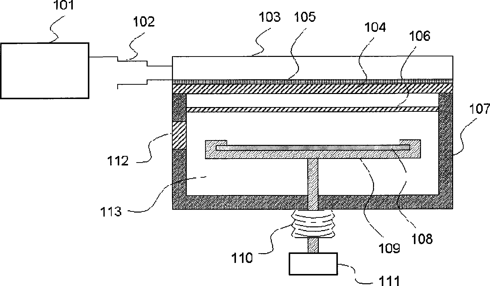
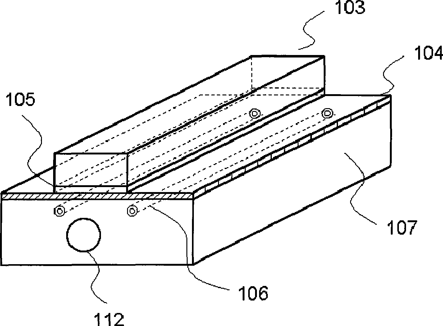
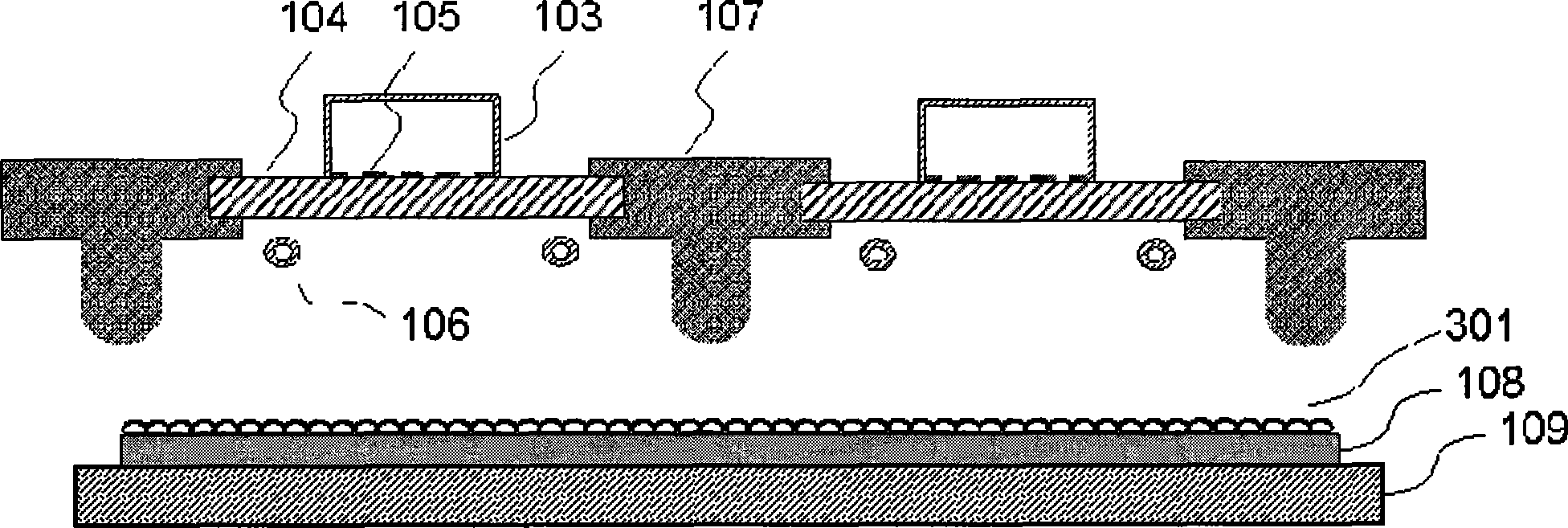
[0035] Figure 7 It is a structural schematic diagram of an embodiment of the thin film preparation device of the present invention. The microwave generated by the microwave source 101 is effectively introduced into the parallel rectangular waveguide 103 through the tapered waveguide 102. The tapered waveguide is also called a waveguide horn, and the microwave can be transmitted from the microwave generator Coupled into the waveguide with a small mismatch loss. The side-by-side rectangular waveguides 103 feed microwaves into the main chamber 113 through the replaceable microwave feeding window and the quartz glass plate 104, and in the main chamber 107, the precursor gas introduced by the gas distribution pipe 106 is excited to generate plasma, and on the substrate 108 Deposit thin films. The purpose of distributing the waveguides side by side is to excite uniform plasma in a large area to achieve the uniformity of large area film deposition.

[0036] The side-by-side rectan...


PUM


Abstract

The invention relates to a large-area microwave plasma chemical vapor deposition device, in particular to the filed of solar batteries and panel display by using the film preparation device to quickly deposit amorphous silicon and microcrystallizing silicon films on a substrate. The device comprises a microwave source, a tapered wave pipe and a rectangle wave pipe; the tapered wave pipe is connected with the microwave source and the rectangle wave pipe; a main cavity with one upper end that is sealed by a quartz glass plate is arranged below the rectangle wave pipe; a microwave feed-in window is positioned between and adheres to the rectangle wave pipe and the quartz glass plate; at least one gas distribution pipe is disposed inside the main cavity; and the main cavity is internally provided with an object load device for loading the substrate and a vacuum system connected with the main cavity body. The rectangle wave pipe is disposed to correspond to the substrate. A large area of uniform plasma is produced by using parallel distribution of pipes, and the device in the invention can realize the homogenization of the large-area film deposition.

Description

technical field [0001] The invention relates to a microwave plasma chemical vapor deposition device, in particular to a large-area microwave plasma chemical vapor deposition device. Background technique [0002] Chemical vapor deposition is a process of depositing a film on a substrate through a chemical reaction between gaseous precursors, and it is widely used in the industry. During the chemical vapor deposition process, the gaseous precursor reacts in the chamber and grows a film on the substrate. Except for the solid state of the film, other products must be gaseous to be taken away by the air flow. In order to form a good The binding force of the film and the substrate material must be low enough, otherwise it is easy to form a low-density film. A typical chemical vapor deposition process is to expose the substrate to one or more different precursors (gaseous substances), a chemical reaction occurs on the surface of the substrate to produce a thin film to be deposited...

Claims


Application Information

Patent Timeline
Patent Type & Authority Applications(China)
IPC IPC(8): C23C16/24C23C16/513
Inventor 王晓飞王志毅丰平王鸿夏芃范振华范继良
Owner 上海拓引数码技术有限公司
Why Eureka
Try Eureka