Electrode construction for enhancing photoelectric transforming efficiency of silicon solar cell

A technology for crystalline silicon solar cells and photoelectric conversion efficiency, applied in circuits, electrical components, semiconductor devices, etc., can solve the problem of reducing the photoelectric conversion efficiency of crystalline silicon solar cells, affecting the photoelectric conversion efficiency of crystalline silicon solar cells, and the photoelectric conversion efficiency of crystalline silicon solar cells. To solve the problems of large surface ratio, etc., to achieve the effect of facilitating interconnection, increasing arrangement density, and reducing series resistance

Inactive Publication Date: 2009-07-15
JIAWEI SOLAR WUHAN
View PDF0 Cites 28 Cited by
  • Summary
  • Abstract
  • Description
  • Claims
  • Application Information

AI Technical Summary

Problems solved by technology

[0003] 1. Due to the dense arrangement of sub-grid lines, the proportion of main and sub-grid lines blocking the light-receiving surface of crystalline silicon solar cells is relatively large, which reduces the light-receiving area of ​​crystalline silicon solar cells and affects the photoelectric conversion efficiency of the entire crystalline silicon solar cells
[0004] 2. Due to the limitation of printing technology, the resistance of metal grid lines in the prior art is relatively high, resulting in a decrease in the photoelectric conversion efficiency of crystalline silicon solar cells

Method used


Image

  • Electrode construction for enhancing photoelectric transforming efficiency of silicon solar cell

Examples


Embodiment Construction

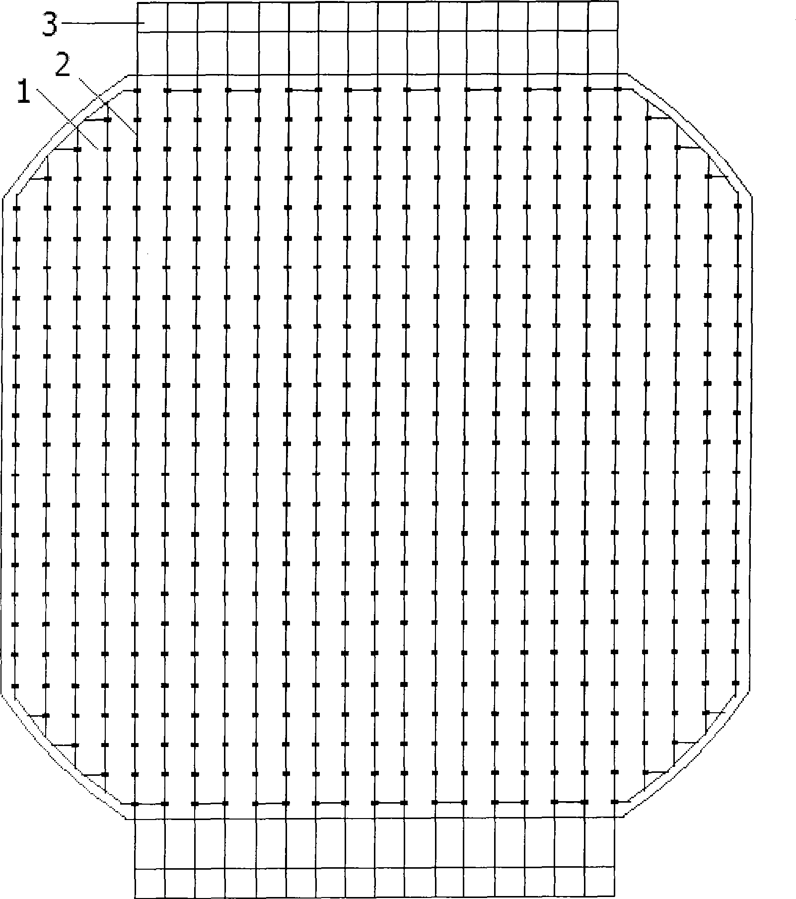
[0015] see figure 1 In this embodiment, a 125mm×125mm quasi-square battery is taken as an example. On the light-receiving surface of a crystalline silicon solar cell substrate, metal grid electrodes 2 arranged in parallel at a distance of 5 mm are arranged. Each metal grid electrode 2 is connected to the silicon solar cell substrate. At least two solder joints 1 are arranged between the light-receiving surfaces, and the distance between two adjacent solder joints 1 is 5 mm. The metal grid line 2 is silver-plated copper wire, and its resistivity is 1.7×10 -8 ohm m. On the side of the crystalline silicon solar cell substrate, there is a bus strip 3 welded to the lead end of the metal grid wire electrode 2. The bus strip 3 is a conductive metal strip. When another single solar cell is connected to it, only another The back electrode of the single solar cell can be welded to it.

[0016] The total number of solder joints in this embodiment is 585, and the density is 4 / cm 2 . T...


PUM


Abstract

The invention discloses an electrode structure for improving a crystal silicon solar battery photoelectric transformation efficiency characterized by arranging parallely set gate lines on a light interception face of the crystal silicon solar battery substrate, and arranging at least two solder joints between each gate line and the crystal solar battery substrate light interception face, wherein the gate lines are conductive gate lines. The invention cancels split-gate lines in a background technique, uses the solder points between the metal gate lines and the crystal solar battery substrate to gather light currents of the crystal silicon solar battery light interception face and guides the currents gathered by the solder points by using the metal gate lines. Because said structure, the invention not only reduces a lightproof area of the light interception face gate line of the crystal silicon solar battery, but also reduces a series resistance of the crystal silicon solar battery, thereby improving the conversion efficiency of the crystal silicon solar battery and facilitating the interconnect of multi-block single batteries.

Description

technical field [0001] The invention relates to a silicon solar cell, in particular to an electrode structure for improving the photoelectric conversion efficiency of a crystalline silicon solar cell. Background technique [0002] At present, the grid lines on the light-receiving surface of a typical crystalline silicon solar cell are composed of main grid lines and sub-grid lines. The main grid lines and fine grid lines are printed on the surface of the cell by screen printing technology. The current of the grid line outputs the power generated by the battery substrate. The gate line structure has the following disadvantages: [0003] 1. Due to the dense arrangement of sub-grid lines, the proportion of main and sub-grid lines blocking the light-receiving surface of crystalline silicon solar cells is relatively large, which reduces the light-receiving area of ​​crystalline silicon solar cells and affects the photoelectric conversion efficiency of the entire crystalline sili...

Claims


Application Information

Patent Timeline
Patent Type & Authority Applications(China)
IPC IPC(8): H01L31/0224H01L31/042
Inventor 丁孔贤李化铮丁孔奇
Owner JIAWEI SOLAR WUHAN
Why Eureka
Try Eureka