Integrated semiconductor light emitting device and method for manufacturing same

A technology for light-emitting devices and semiconductors, which is applied in the manufacture of semiconductor/solid-state devices, semiconductor devices, and electric solid-state devices, etc., can solve the problems of overall aging of the device, low current injection efficiency of light-emitting devices, etc., and achieves improved integration density, sufficient heat dissipation, The effect of excellent reliability

Inactive Publication Date: 2009-07-15
MITSUBISHI CHEM CORP
View PDF4 Cites 18 Cited by
  • Summary
  • Abstract
  • Description
  • Claims
  • Application Information

AI Technical Summary

Problems solved by technology

In this case, current not only flows from the n-side electrode to the nearest p-side electrode, but also flows from one n-side electrode to all p-side electrodes, and the overall current injection efficiency of the light emitting device is not high.
In addition, since all the p-side electrodes and all the n-side electrodes are electrically connected to each other, aging at one place will cause aging of the entire device
Therefore, this type of device is not essentially a large-area surface-oriented light source

Method used


Image

  • Integrated semiconductor light emitting device and method for manufacturing same
  • Integrated semiconductor light emitting device and method for manufacturing same
  • Integrated semiconductor light emitting device and method for manufacturing same

Examples


Embodiment

[0812] Examples are given below to describe the features of the present invention more specifically. The materials, usage amounts, proportions, treatment contents, treatment procedures and the like shown in the following examples can be appropriately changed within the scope not departing from the gist of the present invention. Therefore, the interpretation of the scope of the present invention should not be limited to the specific examples shown below. In addition, in the drawings referred to in the following embodiments, there are parts whose dimensions are changed to facilitate understanding of the structure, and the actual dimensions are as follows.

[0813] "

Embodiment A-1

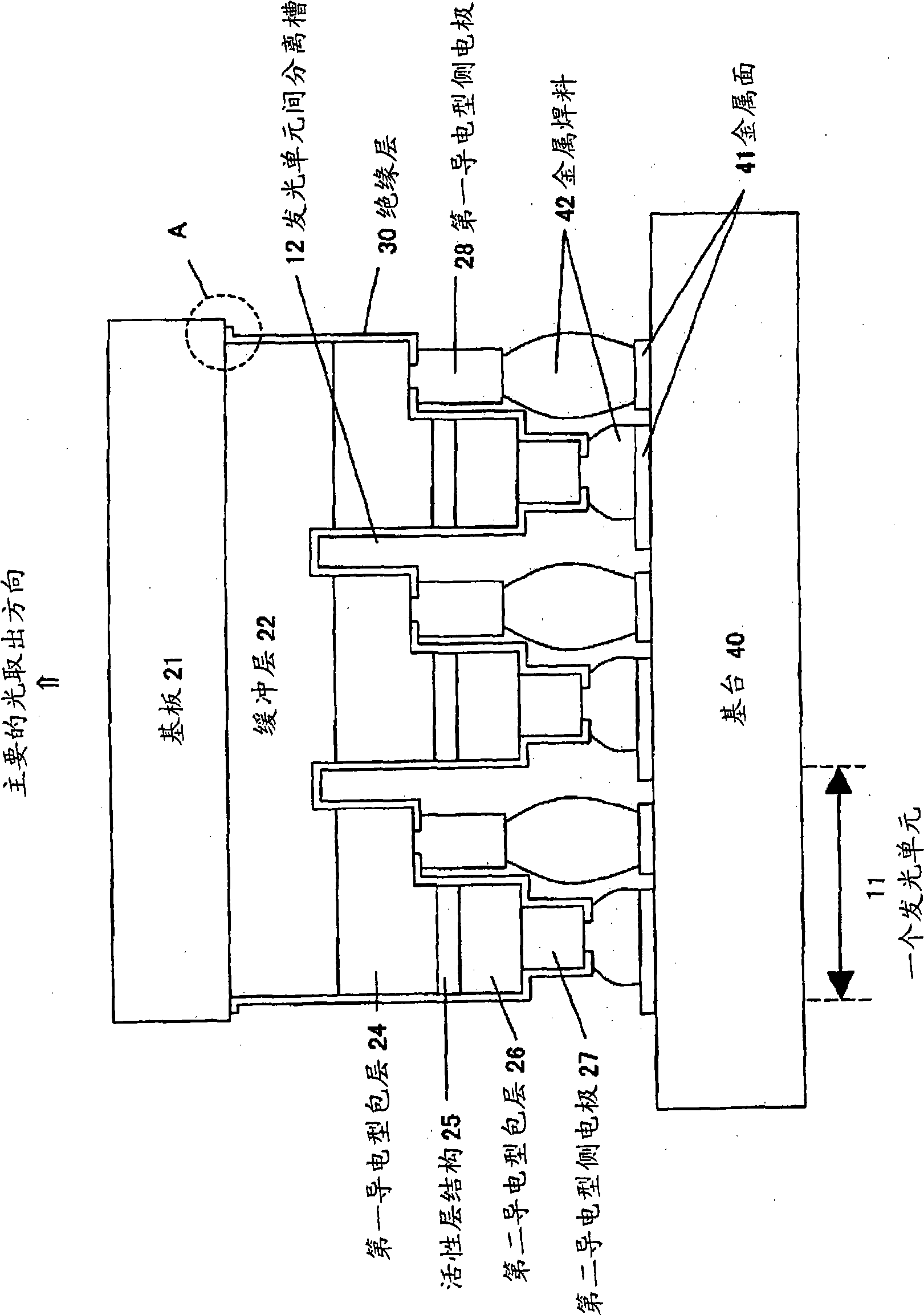
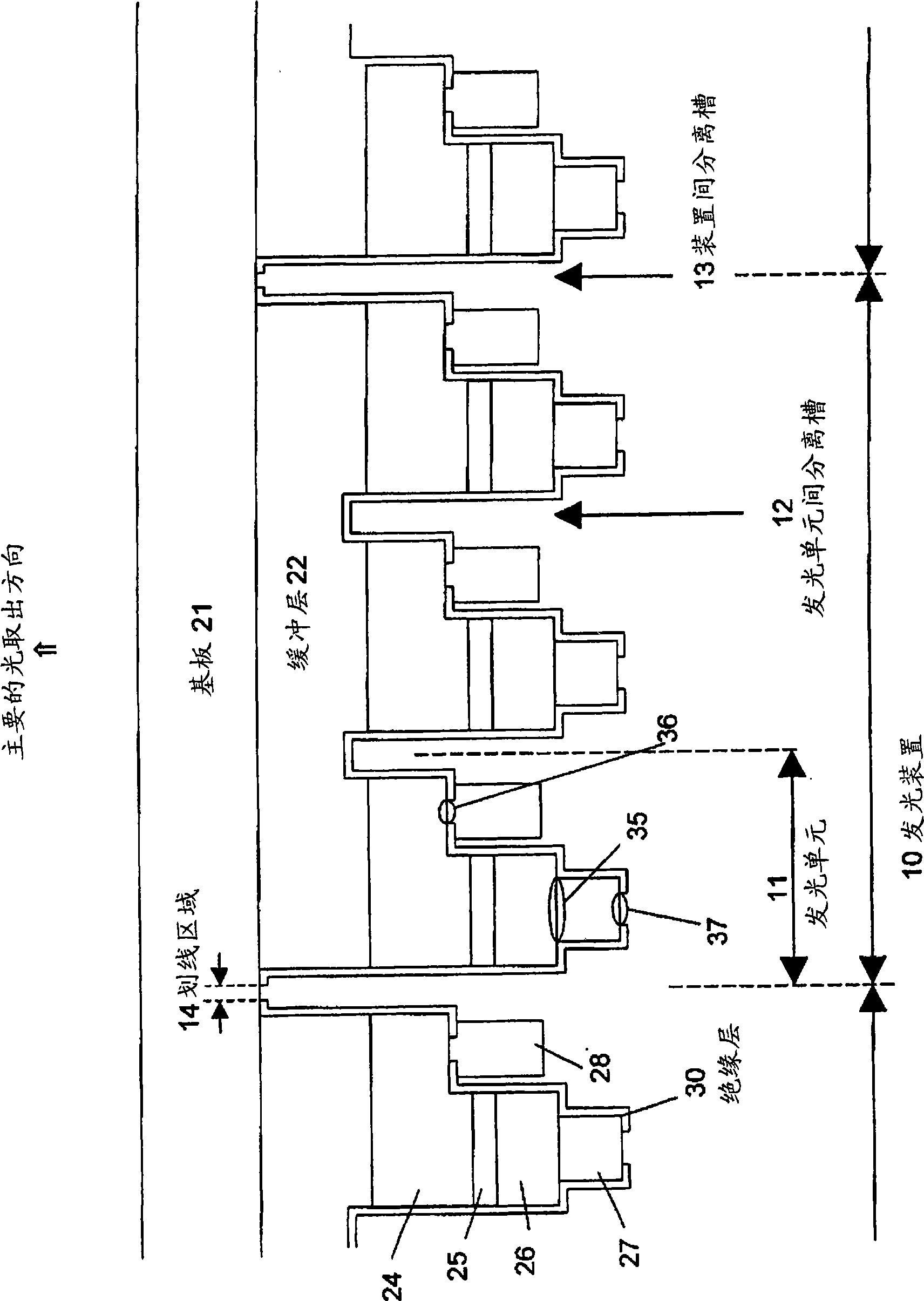
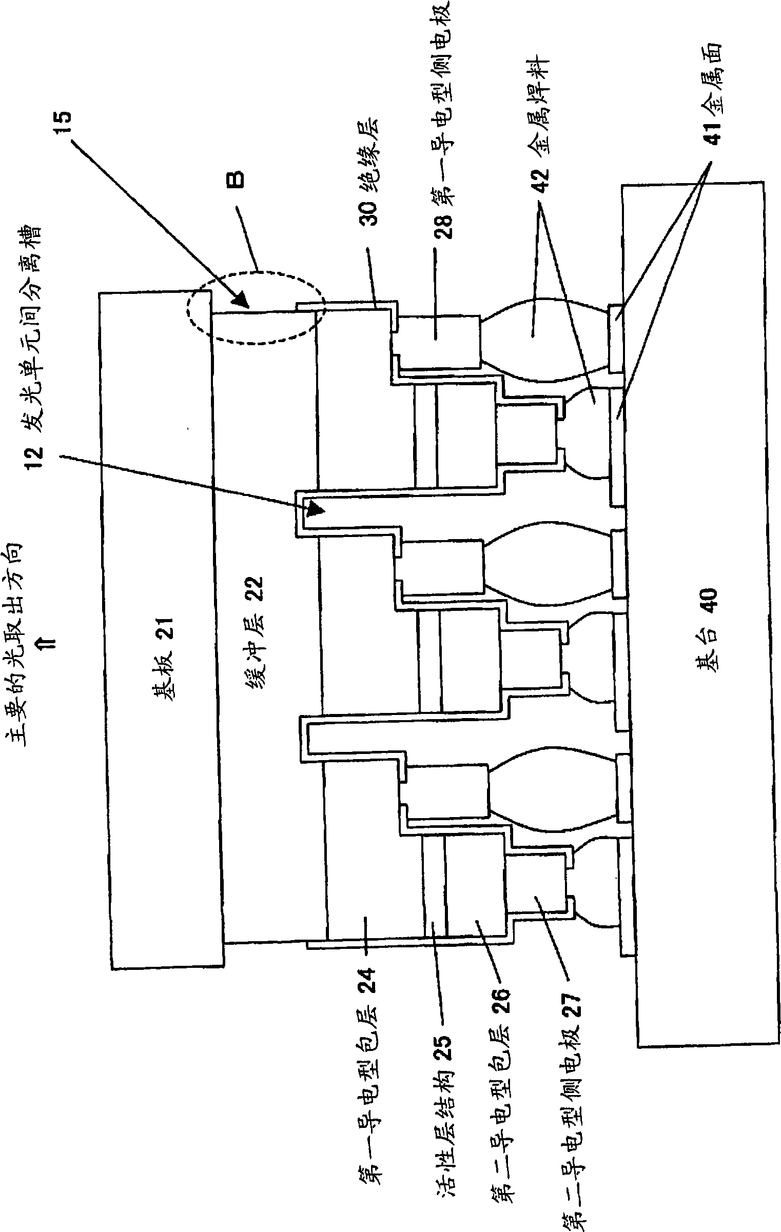
[0815] Make in the following order Figure 1-15 The semiconductor light-emitting device shown. Relevant process diagram reference Figure 1-6 ~ 10, 12 and 14.

[0816] Prepare a c+ plane sapphire substrate 21 with a thickness of 430 μm. First, a 10 nm thick undoped GaN layer grown at a low temperature is formed on it by MOCVD as the first buffer layer 22a, and then a 4 μm thick undoped GaN layer is formed at 1040° C. The doped GaN layer serves as the second buffer layer 22b.

[0817] Further, Si doping (Si concentration 1×10 18 cm -3 ) GaN layer as the first conductivity type (n-type) second cladding layer 24b, with Si doping (Si concentration 3×10 18 cm -3 ) GaN layer as the first conductivity type (n-type) contact layer 24c, and further Si-doped (Si concentration 1.5×10 18 cm -3 ) Al 0.15 Ga 0.85 The N layer serves as the first conductivity type (n-type) first cladding layer 24a. Next, as the active layer structure 25, a barrier layer and a quantum well layer were...

Embodiment A-2

[0837] As in Example A-1, wherein the film formation of the thin-film crystal layer after the buffer layer 22 was formed was performed as follows, and Example A-1 was repeated. That is, in Example A-1, after forming undoped GaN with a thickness of 4 μm as the second buffer layer 22 b at 1040° C., Si doping (Si concentration 5×10 18 cm -3 ) GaN layer as the first conductivity type (n-type) second cladding layer 24b, with Si doping (Si concentration 8×10 18 cm -3 ) GaN layer as the first conductivity type (n-type) contact layer 24c, and further Si-doped (Si concentration 5.0×10 18 cm -3 ) Al 0.10 Ga 0.90 The N layer serves as the first conductivity type (n-type) first cladding layer 24a. Next, barrier layers and quantum well layers are alternately formed to form an active layer structure 25, wherein the barrier layer is an undoped GaN layer formed at 850°C with a thickness of 13nm, and the quantum well layer is formed at 720°C with a thickness of 2nm undoped In 0.1 Ga 0...


PUM


Abstract

Provided is an integrated compound semiconductor light emitting device structure suitable for large-area light emission such as of a surface light source. A method for manufacturing such structure is also provided. The light emitting device is provided with a plurality of light emitting units (11) formed on a transparent substrate (21). The light emitting units are provided with thin film crystal growing layers (24, 25, 26) and first and second conductivity type side electrodes (27, 28). A light extracting direction is on a substrate side, and the first and the second conductivity type side electrodes are formed on a side opposite to the light extracting direction. The light emitting units are electrically separated by a groove (12), which is provided for separating the light emitting units and is formed by removing the thin crystal growing layer, from the surface up to a part of the buffer layer (22).

Description

technical field [0001] The present invention relates to an integrated compound semiconductor light-emitting device, in particular to a light-emitting diode (LED) using GaN-based materials. It is worth noting that, in this specification, the term light emitting diode or LED generally includes light emitting elements such as laser diodes and superluminescent light emitting diodes. Background technique [0002] Conventionally, electronic devices and light-emitting devices using group III-V compound semiconductors are known. In particular, light-emitting devices have realized red light emission using AlGaAs-based materials or AlGaInP-based materials formed on GaAs substrates, orange or yellow light emission using GaAsP-based materials formed on GaP substrates, and the like. In addition, an infrared light-emitting device using an InGaAsP-based material on an InP substrate is also known. [0003] As the form of these devices, there are known light emitting diodes (light emitting...

Claims


Application Information

Patent Timeline
Patent Type & Authority Applications(China)
IPC IPC(8): H01L33/00H01L21/3065
CPCH01L27/153H01L2224/16225H01L2224/1403
Inventor 堀江秀善
Owner MITSUBISHI CHEM CORP
Why Eureka
Try Eureka