Standard CMOS fully differential optical detector and manufacturing method thereof

A photodetector and fully differential technology, which is applied in semiconductor/solid-state device manufacturing, radiation control devices, electrical components, etc., can solve problems such as asymmetry of input signals, limitation of optical receiver bandwidth and sensitivity, and imbalance of differential branches. , to achieve the effect of improving bandwidth and sensitivity

Inactive Publication Date: 2009-07-22
TIANJIN UNIV
View PDF6 Cites 9 Cited by
  • Summary
  • Abstract
  • Description
  • Claims
  • Application Information

AI Technical Summary

Problems solved by technology

The disadvantage of this structure is that it causes the imbalance of the two differential branches of the differential optical receiver (the differential transimpedance preamplifier and the photodetector are asymmetrically integrated) and the input of the two differential branches of the differential optical receiver The asymmetry of the signal (that is, the input end connected to the photodetector has a photo-generated current signal input, while the other end has no photo-generated current signal input), thus limiting the bandwidth and sensitivity of the optical receiver

Method used


Image

  • Standard CMOS fully differential optical detector and manufacturing method thereof
  • Standard CMOS fully differential optical detector and manufacturing method thereof
  • Standard CMOS fully differential optical detector and manufacturing method thereof

Examples


Embodiment Construction

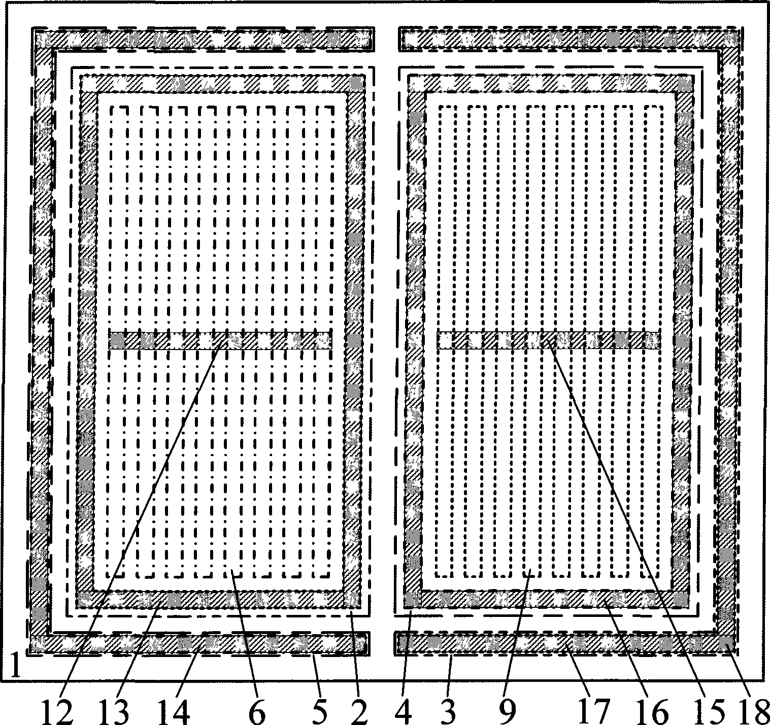
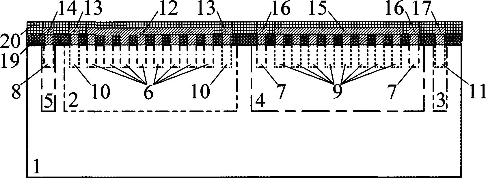
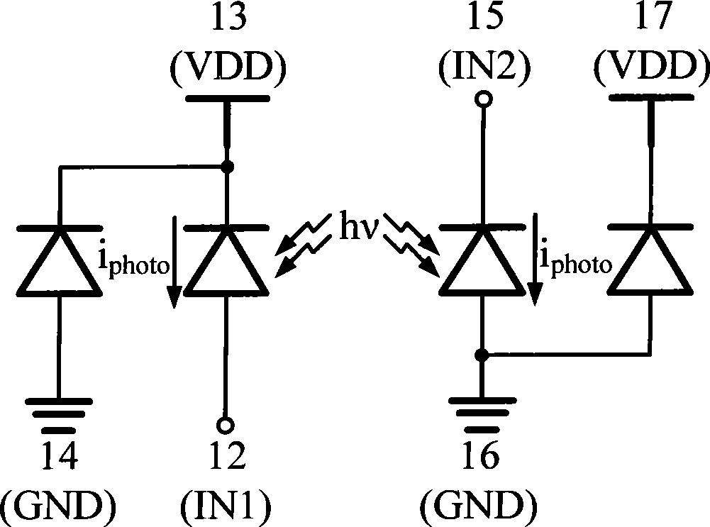
[0025] The present invention is achieved by the following methods: figure 1 It is a top view of the structure of the standard CMOS fully differential photodetector of the present invention; figure 2 It is a structural sectional view of the standard CMOS fully differential photodetector of the present invention along the longitudinal bisector; image 3 is the equivalent circuit model of the standard CMOS fully differential photodetector of the present invention when it works normally. The present invention is described in detail below in conjunction with accompanying drawing and embodiment:

[0026] figure 1 with figure 2 The manufacturing process flow of the standard CMOS fully differential photodetector shown is as follows:

[0027] First, a rectangular deep N well region 2 and a concave deep N well region 3 as well as a rectangular high voltage P well region 4 and a concave high voltage P well region 5 are sequentially fabricated on a P-type substrate 1 . Among them, ...


PUM


Abstract

The invention relates to a standard CMOS fully-differential optical detector, belonging to the field of optical communication system and optical interconnection. The optical detector has functions of converting optical signals input by the same optical fiber into a pair of fully-differential current signals and providing a pair of symmetrical and consistent input loads for a subsequent differential receiver circuit. The optical detector comprises an interdigitating P+/deep N well/high voltage P well type photodetector and an interdigitating N+/high voltage P well/deep N well type photodetector; wherein, the two photodetectors share the same shape and size and are symmetrical and tightly close to each other, in addition, the two photodetectors take up half of the total light-emitting area and form a light-emitting area similar to a square. The optical detector of the invention can overcome the defect that the input loads of the existing differential optical receiver are unsymmetrical and greatly improve the bandwidth and sensitivity of the existing differential optical receiver.

Description

technical field [0001] The invention belongs to the field of optical communication system and optical interconnection, and relates to a full differential optical detector fully compatible with standard CMOS technology. Background technique [0002] For optical receivers used in high-speed optical communication applications such as short-distance and very short-distance optical communication, it is not only necessary to use a differential circuit structure to improve circuit stability and overcome various common-mode noise interference, but also to use silicon-based standard CMOS technology To realize the monolithic integration of the optical receiver to greatly reduce its application cost. [0003] The reported standard CMOS differential optoelectronic integrated receiver generally only integrates one photodetector, that is, only one of the two differential branches of the differential transimpedance preamplifier is connected with a photodetector capable of detecting the inp...

Claims


Application Information

Patent Timeline
Patent Type & Authority Applications(China)
IPC IPC(8): H01L27/144H01L21/8238
Inventor 毛陆虹余长亮
Owner TIANJIN UNIV
Why Eureka
Try Eureka