
Production method for printed circuit heat radiation board

A technology of printed circuit and heat sink, applied in the field of manufacturing method of printed circuit heat sink, can solve the problems of fast tool wear, inconsistent with the needs of video and audio data data operation, slow processing speed, etc., so as to achieve slow tool wear and better chip removal effect. Excellent, fast processing effect

Inactive Publication Date: 2009-07-22
SHENQ FANG YUAN TECH
View PDF0 Cites 8 Cited by
  • Summary
  • Abstract
  • Description
  • Claims
  • Application Information

AI Technical Summary

Problems solved by technology

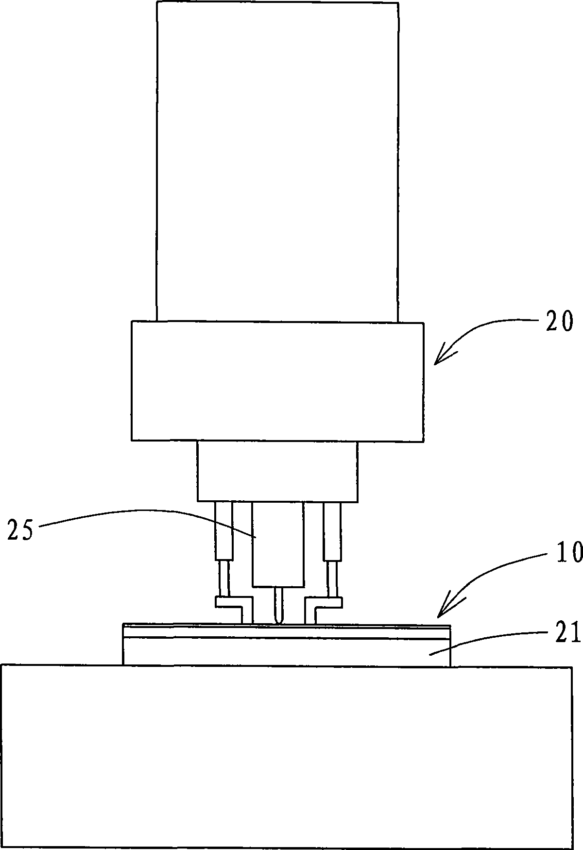
[0005] However, the conventional non-metallic printed circuit board does not have high heat-resistant reliability and safety, so it does not meet the needs of the audio-visual data calculation of high-function information products such as PDAs, mobile phones, and DVs. Therefore, there is a kind of A printed circuit cooling plate with a copper layer compounded on an aluminum substrate was born due to luck, but this printed circuit cooling plate cannot be smoothly processed by the conventional PCB processing special machine 20, which is due to the traditional manufacturing method , because the rigidity and ductility of the latest printed circuit heat sink are much higher than that of the traditional printed circuit board 10, so the conventional PCB processing special machine 20 is processed at a reduced spindle speed of 25, due to the limited torque of 0.2NM (Newton meters ), and the power is only 1.1KW (kilowatt), so it is not enough to process high-quality finished products efficiently, and often cannot process a finished product that meets the quality requirements in one hour, because this traditional method must improve the fixing method of the cooling plate at the same time , The main shaft structure and cooling method of the special machine for PCB processing can successfully overcome the problems of tool vibration, slow processing speed, and fast tool loss caused by processing the cooling plate.

Method used


Image

  • Production method for printed circuit heat radiation board
  • Production method for printed circuit heat radiation board
  • Production method for printed circuit heat radiation board

Examples


Embodiment Construction

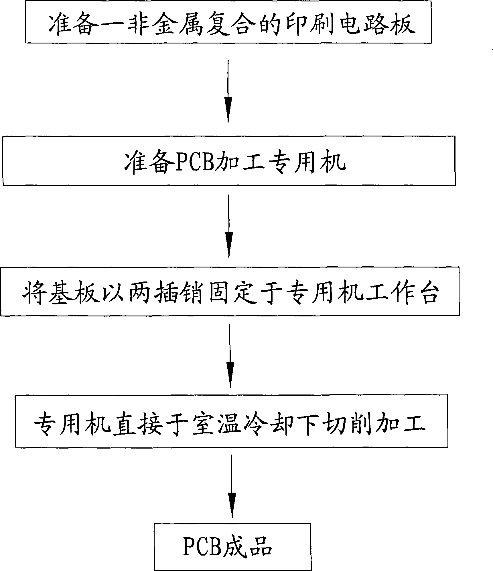
[0046] The present invention relates to a method for manufacturing a printed circuit cooling plate, please refer to Figure 4 Promptly propose the present invention is different from the conventional manufacturing process below, comprises:

[0047] 1. Prepare a composite metal heat sink; Figure 5 As shown, the present invention adopts a metal heat dissipation plate 30 composed of aluminum and copper plates up and down. The aluminum layer 31 of the heat dissipation plate 30 has better heat dissipation and heat resistance effects. As for the surface of the copper layer 32, a wiring circuit pattern 33 is etched. ;

[0048] 2. Vacuum absorb the cooling plate to a carrier with a positioning structure; Figure 5 to Figure 8 As shown, the carrier 40 has a flow channel 41 vertically and horizontally recessed on the top surface, and a leak-proof gasket 42 with a protruding surface is sunk outside the range of the flow channel 41, and then made of acrylic or other plastics. The jig ...


PUM


Abstract

The present invention provides a method for preparing cooling plate of printed circuit. Firstly a double layer metal cooling plate compounding aluminum and copper is firstly prepared, wherein the cooling plate is etched with a wiring circuit pattern on the surface of copper layer. Then the cooling plate is fixed on a platform with a vacuum absorption mode. The platform is installed on a processor and is provided with a positioning structure for locating the cooling plate. The limiting of main shaft of processor has high cutting torsion and strong structural property compared with the known PCB processing special machine. The main shaft can execute cutting to the cooling plate on the platform after assembling the cutter. Simultaneously the cutting position can be executed with temperature dropping and chip removal with a mode of forced cooling for quickly completing the procession of a high-quality cooling plate.

Description

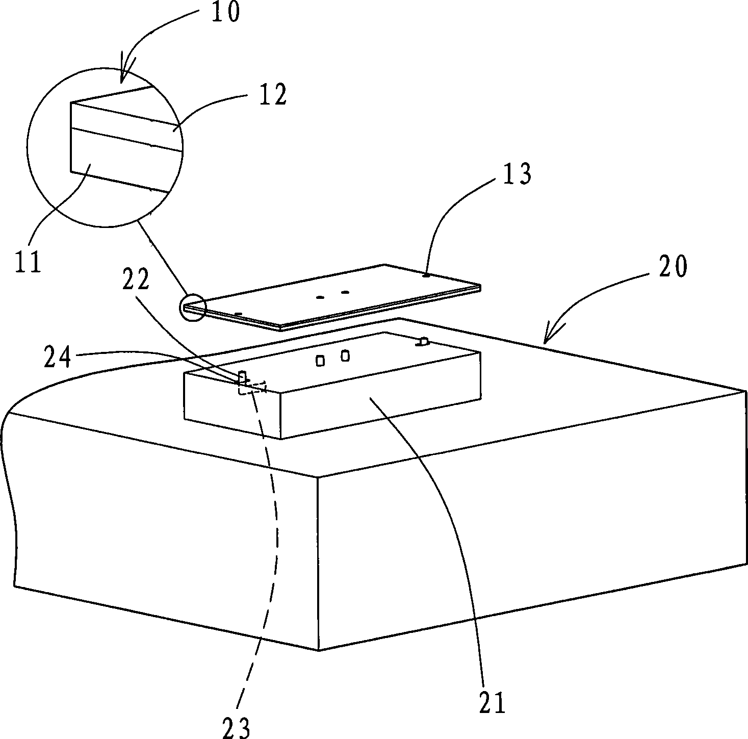
technical field [0001] The invention provides a method for manufacturing a printed circuit cooling plate that conforms to economical principles, effectively improves processing accuracy, and maintains high quality and other expected benefits. Background technique [0002] see figure 1 , 2 As shown, the traditional printed circuit board 10 is mainly composed of a thinner copper layer 12 on a non-metallic substrate 11. The surface of the copper layer 12 is etched with the required layout circuit pattern to form a non-metallic composite printed circuit board. 10. To make it have the characteristics of light weight and low cost; [0003] The printed circuit board 10 is provided with pin holes 13 at both ends, and the PCB processing special machine 20 is protrudingly provided with pins 22 corresponding to the two pin holes 13 on the workbench 21, and one of the pins 22 is oiled. The connecting rod 23 controlled by pressure or air pressure can move along the chute 24 provided o...

Claims


Application Information

Patent Timeline
IPC IPC(8): H05K3/00H05K7/20B23C3/13B23Q11/10
Inventor 石政修
Owner SHENQ FANG YUAN TECH
Learn More