
Noise filter array

A noise filter and filter technology, applied in the direction of inductors, fixed inductors, structurally fixed capacitor combinations, etc., can solve problems such as difficulty in accordance with communication frequency bands, inability to respond appropriately, and achieve easy adjustment and suppression of plating thickness deviations. Effect

Inactive Publication Date: 2009-07-22
MURATA MFG CO LTD
View PDF1 Cites 16 Cited by
  • Summary
  • Abstract
  • Description
  • Claims
  • Application Information

AI Technical Summary

Problems solved by technology

[0009] But, Figure 12 In the noise filter array with the structure shown, the coil L0 of the LC series resonant circuit constituting each filter element is common, and there is only one, so it is difficult to adjust the inductance of the LC series resonant circuit individually for each communication frequency band.
Therefore, when the frequency of the noise to be removed by each filter element is different, there is a problem that it cannot be properly dealt with.

Method used


Image

  • Noise filter array
  • Noise filter array
  • Noise filter array

Examples


Embodiment 1

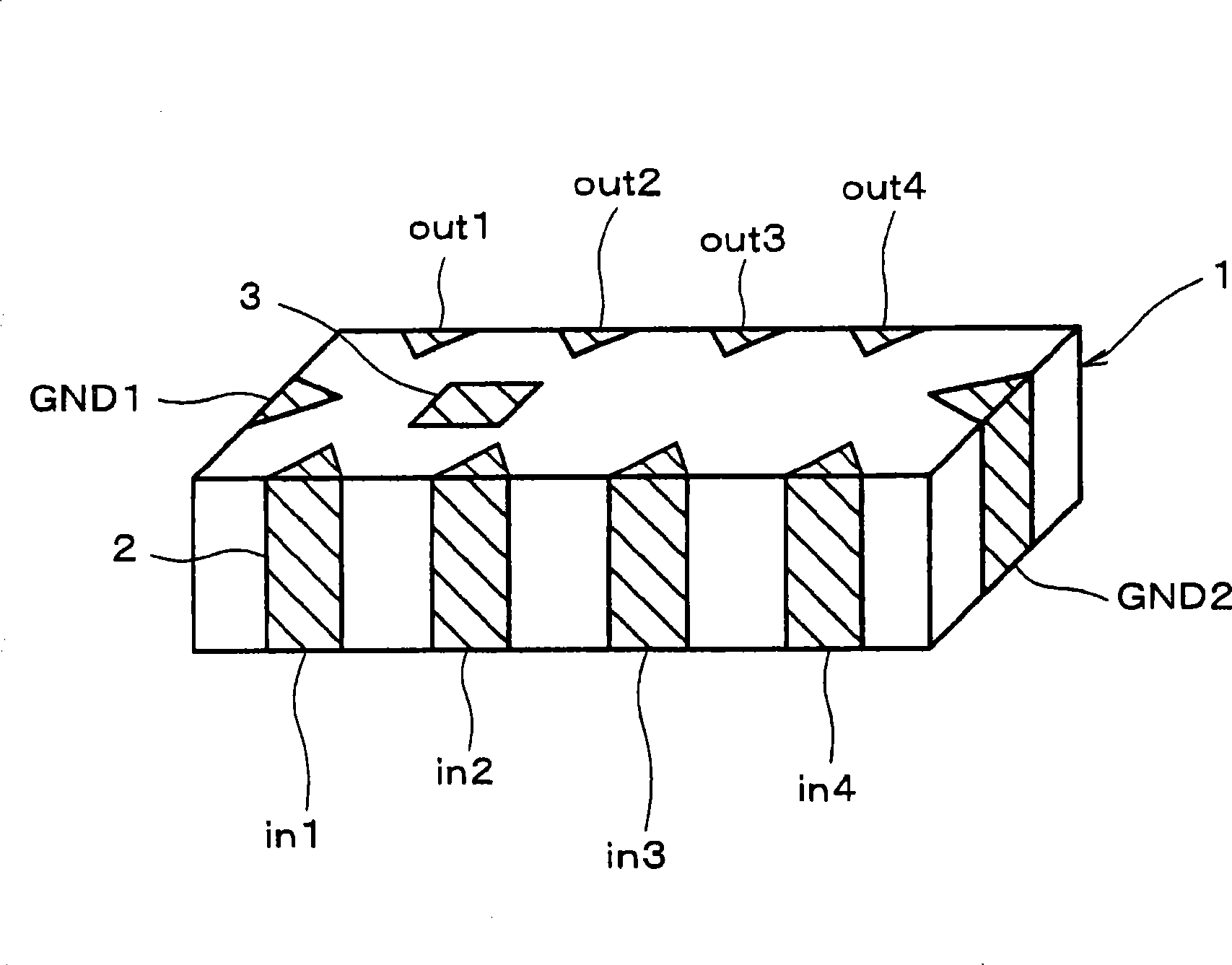
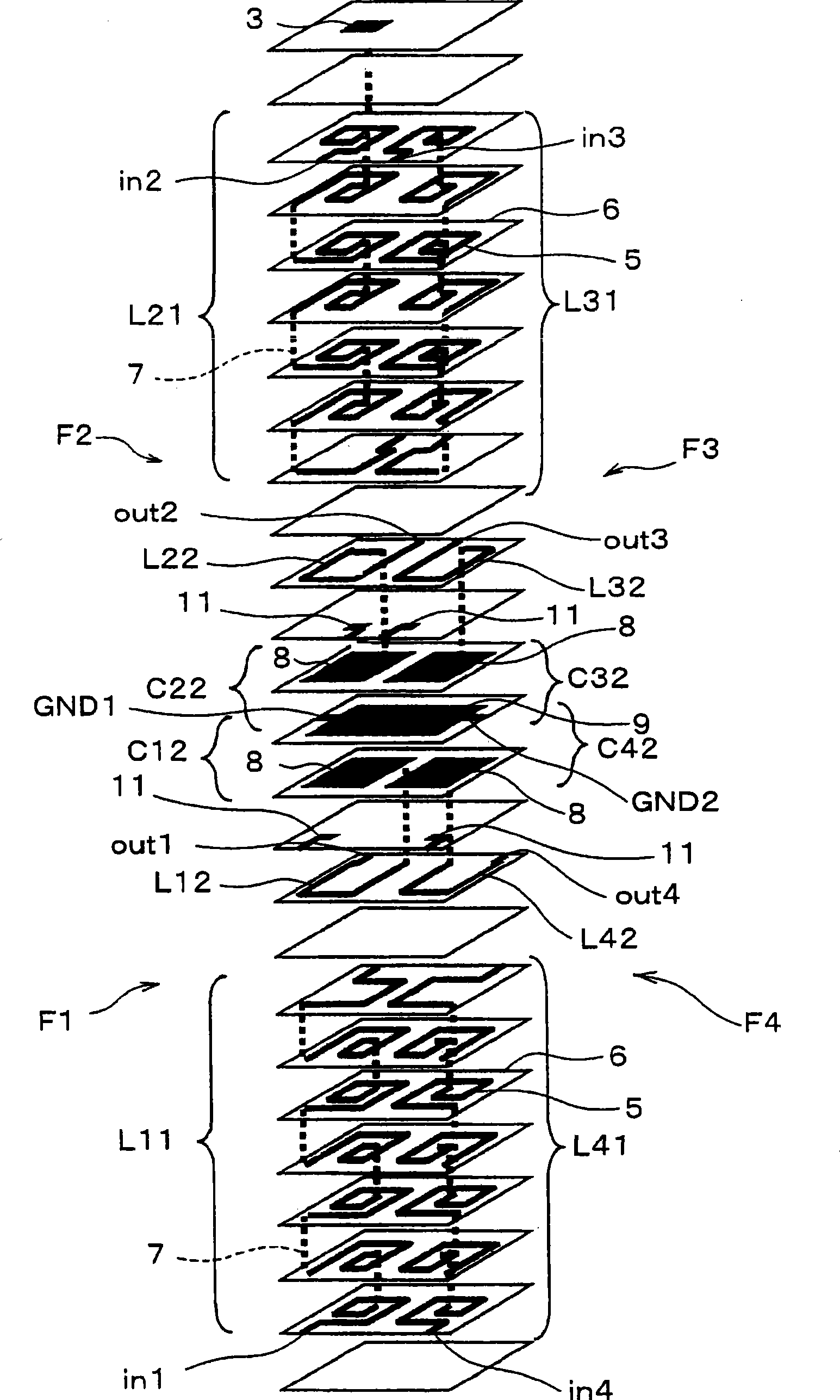
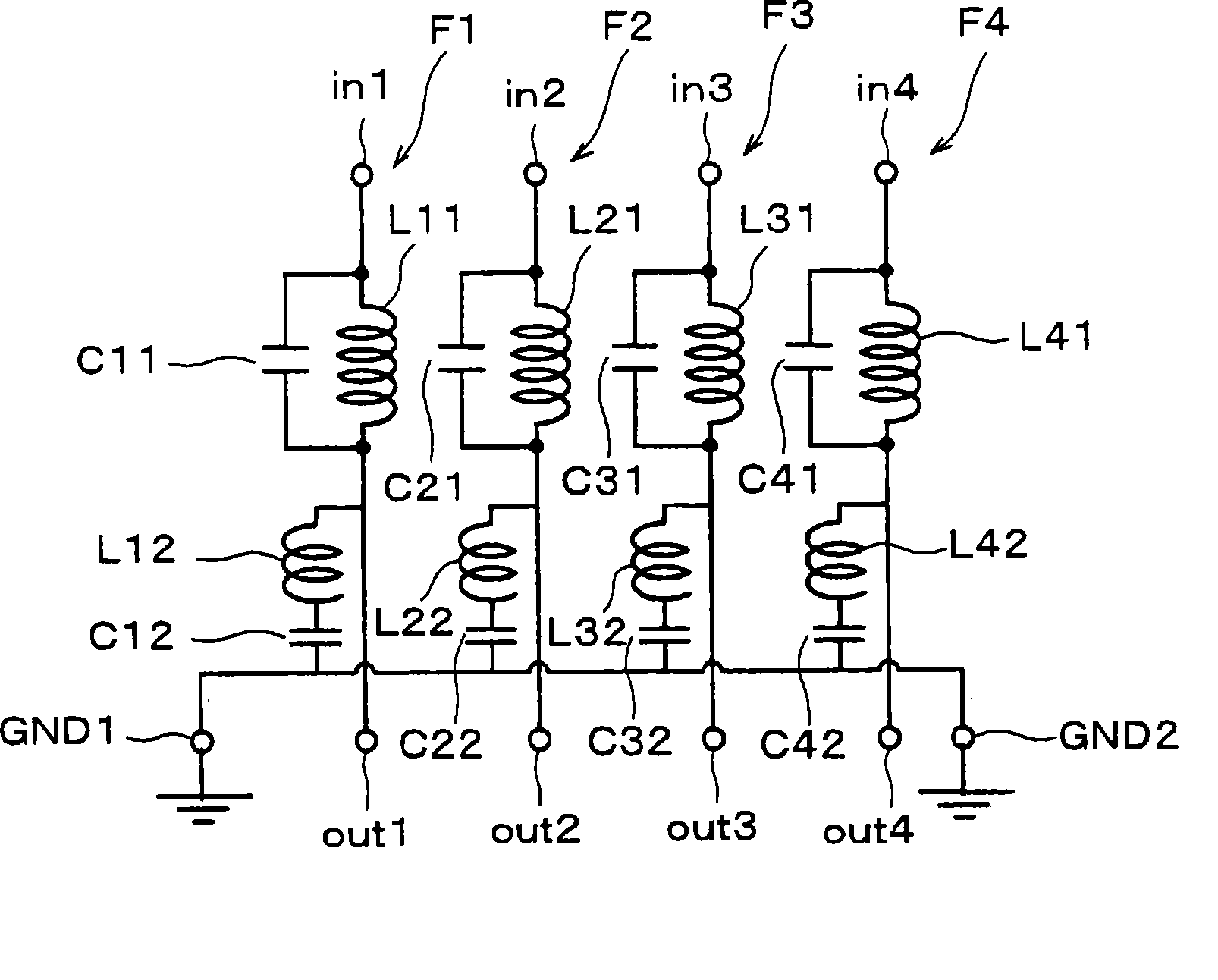
[0068] figure 1 is a perspective view showing the appearance of the noise filter array according to Embodiment 1 of the present invention, figure 2 is an exploded perspective view of the noise filter array, image 3 is the electrical equivalent circuit diagram of the noise filter array, Figure 4 With figure 2 The exploded perspective view of the corresponding reconfiguration image 3 The electrical equivalent circuit diagram of the electrical equivalent circuit diagram.

[0069] Below, refer to Figure 1 ~ Figure 4 , to illustrate the noise filter array of Embodiment 1.

[0070] The noise filter array of the present embodiment 1 includes a rectangular parallelepiped laminated body 1 in which rectangular insulating sheets made of a ceramic dielectric material such as barium titanate or a ceramic magnetic material such as ferrite are stacked and fired as a whole. . In addition, external electrodes 2 for forming terminals are formed on the peripheral side of the lamina...

Embodiment 2

[0094] Figure 7 It is an exploded perspective view of the noise filter array according to Embodiment 2 of the present invention. In addition, in Figure 7 in, with Figure 1 ~ Figure 4 Portions assigned the same symbols represent the same or corresponding portions as the structure of Example 1.

[0095] In the noise filter array of the second embodiment, the respective inductance adjustment conductors L12 to L42 are formed in approximately the same shape so that the inductance values ​​of the LC series resonant circuits SR1 to SR4 of the respective filter elements F1 to F4 are equal to each other. elements all become the same value. Also, in Example 2, as in Example 1, two filter elements F2, F3 and F1, F4 are integrally formed on both sides in the thickness direction (lamination direction) of the ground-side electrode 9 as a boundary.

[0096] In the noise filter array of the second embodiment, the inductance adjustment conductors L12 to L42 are individually provided for...

Embodiment 3

[0101] Figure 9 It is an exploded perspective view of the noise filter array according to Embodiment 3 of the present invention. In addition, in Figure 9 in, with Figure 1 ~ Figure 4 Portions assigned the same symbols represent the same or corresponding portions as the structure of Example 1.

[0102] In the noise filter array of Embodiment 3, the inductance adjustment conductors L12 to L42 constituting the LC series resonance circuits SR1 to SR4 and the signal-side electrodes 8 of the capacitors C12 to C42 are integrally formed on the same surface, that is, formed on a single surface. On the insulating sheet 6. Also, in the noise filter array of the third embodiment, as in the first embodiment, the ground-side electrode 9 is used as a boundary, and two filter elements F2, F2, and F3 and F1, F4.

[0103] As in the case of Embodiment 3, the inductance adjustment conductors L12-L42 and the signal-side electrode 8 of the capacitor are integrally formed in advance on an in...


PUM


Abstract

Provided is a noise filter array wherein inductances of LC serial resonance circuits of a plurality of filter elements can be independently adjusted while maintaining a simple configuration as a whole. The filter elements (F1-F4) composed of an LC parallel resonance circuit and the LC serial resonance circuit, which have coils and capacitors, are arranged in parallel in an array and integrally formed. Inductance adjusting conductors (L12-L42), which configure the LC serial resonance circuit with grounding capacitors (C12-C42), which configure the filter elements (F1-F4), are separately connected to the signal side electrode (8) of the capacitors (C12-C42). A grounding side electrode (9) of the capacitors (C12-C42) are arranged to commonly face the signal side electrodes (8).

Description

technical field [0001] The present invention relates to a noise filter array integrally formed by arranging a plurality of filter elements including LC parallel resonant circuits and LC series resonant circuits having coils and capacitors in an array. Background technique [0002] For example, there are various communication methods (GSM method, DCS method, PCS method, etc.) in mobile phones, so a plurality of communication frequency bands have been used in a single mobile phone in the past. In this case, in order to prevent the reception sensitivity of each communication frequency band from deteriorating, it is necessary to effectively remove noise in each communication frequency band. [0003] As an example, after removing noise in each communication frequency band around 900 MHz or around 1.8 GHz, the noise filter is required to obtain attenuation over a wide range in each communication frequency band. In order to configure a filter having such a wide attenuation charact...

Claims


Application Information

Patent Timeline
IPC IPC(8): H03H7/01H01F17/00H01F27/00H01G4/40
Inventor 佐佐木友嘉羽田野研次郎上野治彦
Owner MURATA MFG CO LTD
Learn More