Light source structure based on LED

A technology of light-emitting diodes and light sources, which is applied in the direction of light sources, point light sources, components of lighting devices, etc., can solve problems such as difficult to achieve uniform light-emitting mode, serious loss of light energy, uneven brightness, etc., to achieve the solution of LED light-emitting energy Low utilization rate, easy to clean, solve the effect of uneven brightness

Inactive Publication Date: 2009-07-29
TSINGHUA UNIV
View PDF4 Cites 5 Cited by
  • Summary
  • Abstract
  • Description
  • Claims
  • Application Information

AI Technical Summary

Problems solved by technology

Statistical astigmatism uses specific distribution of astigmatism particles or irregular rough surfaces (such as frosted glass) to achieve astigmatism. The configuration curve of the lens unit is often a simple curve such as an arc or a parabola. There are serious problems in the astigmatism plate with this structure: because the configuration of the concave-convex lens unit has not been systematically designed, the brightness uniformity is not good when emitting light, and the utilization of LED luminous energy The rate is generally not high
[0005] The astigmatism plate provided by the patent WO2008 / 134018 realizes astigmatism by connecting two layers of concave lens arrays whose main axis directions are staggered with optical glue in the middle. The concave lens structure is obtained by simple parameter fitting, and it is difficult to achieve uniform light emission and its astigmatism angle is only + / -30°. In order to achieve large-angle astigmatism, multi-layer structures are often used, which is not advantageous in terms of cost and astigmatism effect; the configuration curve of the micro-convex lens array of the astigmatism plate provided by the patent US7092166B1 It is obtained by simple parameter fitting, but because it is a multi-layer structure, it also has similar shortcomings and is difficult to be practical
[0006] In addition, currently published light source structure patents generally have the problem of low energy utilization
In patent CN101208557A, a direct lighting device is formed by arranging a diffusion plate with an integrated cylindrical lens array on the surface and a back surface on a box-shaped light reflection plate with a light source inside. However, the two-layer cylindrical lens without system design The simple structure determines that it has a serious reverse total reflection problem. Most of the light emitted from the LED can only be emitted after multiple reflections and refractions between the diffuser plate and the light reflector plate, and more than one optical lens is set on the light diffuser plate. film, the light transmittance is low, and the loss of light energy is serious; the structure of the light source provided by the patent CN101188261A is characterized in that: the emitted light of the LED chip and the light reflected by the reflective cup pass through the diverging lens to form uniformly distributed divergent light, and then form Evenly emitted flat light, but it does not provide a designed diffuser, which greatly reduces the utilization rate of LED luminous energy
[0007] In order to solve the problems of low light energy utilization rate and uneven brightness of the existing LED-based light source structure, we invented a LED-based light source structure, which contains the light-emitting processing unit of the LED chip and the optical fiber designed by the non-imaging optical design method. Astigmatism plate, which has the advantages of comfortable human eyes, environmental friendliness, and high utilization rate of LED luminous energy

Method used


Image

  • Light source structure based on LED
  • Light source structure based on LED
  • Light source structure based on LED

Examples


Embodiment Construction

[0044] The present invention will be further elaborated below in conjunction with the accompanying drawings and embodiments.

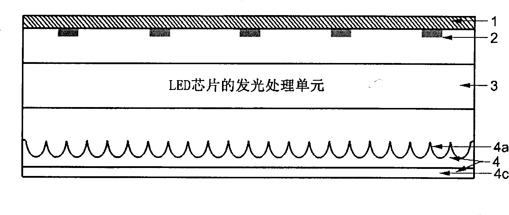
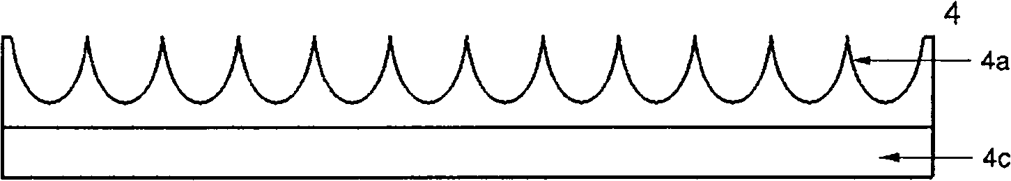
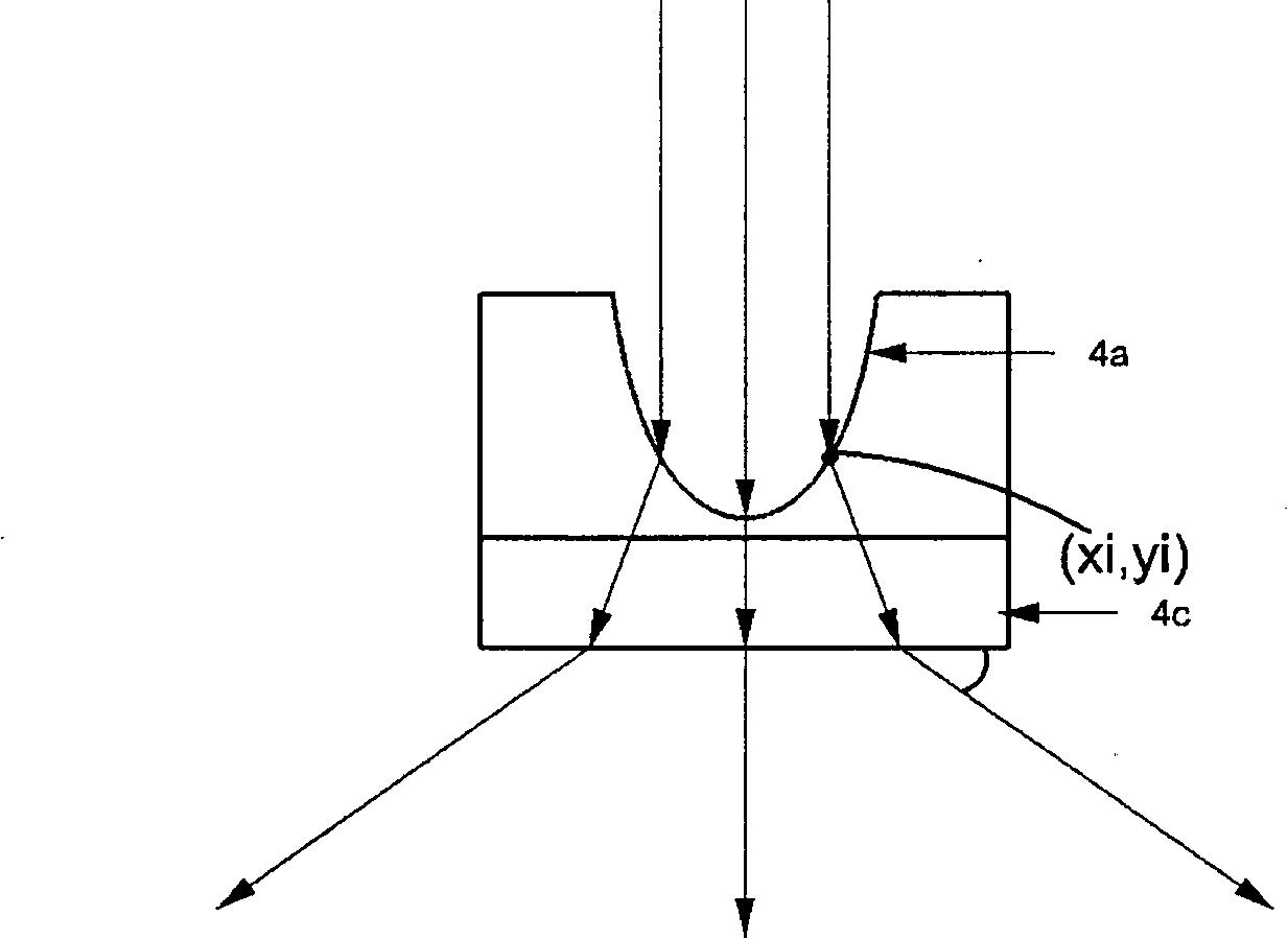
[0045] The basic structure of the light source structure device disclosed in the present invention is as follows: figure 1 shown. The light source structure at least includes a substrate 1, an LED chip 2, a light emitting processing unit 3 of the LED chip, and an optical diffuser plate 4 with non-imaging optical design. The LED chip 2 fixed on the substrate 1 is a light source, and its light field distribution is transmitted to the inner surface of the optical astigmatism plate 4 after being processed by the light emission processing unit 3 of the LED chip, including but not limited to collimation; the optical astigmatism plate 4 At least one side contains engineered microstructures that scatter incident light to form a light source structure of uniform brightness.

[0046] At least one side of the optical astigmatism plate of the present invention i...


PUM


Abstract

The invention relates to a light source structure based on a light emitting diode (LED), which belongs to the technical field of LED application. The light source structure at least comprises a baseplate 1, an LED chip 2, a light-emitting processing unit 3 of the LED chip and an optical light scattering plate 4 designed by nonimaging optics, wherein, the LED chip 2 fixed on the baseplate 1 is the light-emitting source, the optical field distribution is processed by the light-emitting processing unit 3 of the LED chip including but not limited to on and then transmitted to the inner surface of the optical light scattering plate 4; at least one side of the optical light scattering plate 4 comprises a microstructure designed by nonimaging optics, the microstructure ensures the incident light to scatter, thus a light source structure with uniform luminance is formed. The light source structure provided by the invention has the advantages of comfort for human eyes, friendly environment and high utilization rate of the LED luminous energy; the structure can be made into flat shapes including but not limited to squareness, roundness, ellipse, sphericity, spheroidicity, and the like, and non-flat shapes including but not limited to spherical surface, ellipsoidal surface, cylindrical surface and the like, which can realize infinite extension.

Description

technical field [0001] The invention relates to a light source structure based on light-emitting diodes (LEDs). The light source structure at least includes a substrate, an LED chip, a light-emitting processing unit for the LED chip, and an optical diffuser plate, and belongs to the technical field of light-emitting diode applications. Background technique [0002] Light Emitting Diode (LED for short) is a solid-state electro-optical conversion conductor device, with potential advantages such as high luminous efficiency, long life, small size, fast response, shock resistance, environmental protection, and safety in use. It is considered to be the third generation of lighting sources after incandescent lamps and fluorescent lamps. [0003] However, the use of LEDs to make light source structures faces many technical barriers. One of the important factors is the glare and uneven brightness caused by the small luminous flux and high brightness characteristics of traditional con...

Claims


Application Information

Patent Timeline
Patent Type & Authority Applications(China)
IPC IPC(8): F21V13/00F21V5/08F21V7/04F21Y101/02
Inventor 罗毅冯泽心韩彦军
Owner TSINGHUA UNIV
Why Eureka
Try Eureka