
Splicing detection device based on minor caliber circular Shack-Hartmann wavefront sensor

A detection device and sensor technology, applied in the field of optical detection, can solve the problems of harsh experimental conditions, lack of universality, and slow detection speed.

Active Publication Date: 2009-07-29
INST OF OPTICS & ELECTRONICS - CHINESE ACAD OF SCI
View PDF0 Cites 29 Cited by
  • Summary
  • Abstract
  • Description
  • Claims
  • Application Information

AI Technical Summary

Problems solved by technology

At the same time, the interferometer splicing detection scheme also has harsh experimental conditions, is sensitive to atmospheric turbulence, temperature, vibration, and noise; needs to readjust the device after each movement, and has limitations such as slow detection speed
[0011] T.D.Raymond, D.R.Neal et al. used a square Hartmann-Shack wavefront sensor to measure the surface topography of Si wafers in "High-speed, non-interferometric nanotopographiccharacterization of Si wafer surfaces," (Proc. SPIE 4809, 2002.208-216). Splicing detection, but a complete general mathematical model suitable for any number of splicing frames has not been constructed, and it lacks universality for domestic and foreign markets that mainly use circular aperture Hartmann

Method used


Image

  • Splicing detection device based on minor caliber circular Shack-Hartmann wavefront sensor
  • Splicing detection device based on minor caliber circular Shack-Hartmann wavefront sensor
  • Splicing detection device based on minor caliber circular Shack-Hartmann wavefront sensor

Examples


Embodiment Construction

[0045] The present invention will be described in detail below in conjunction with the accompanying drawings and specific embodiments.

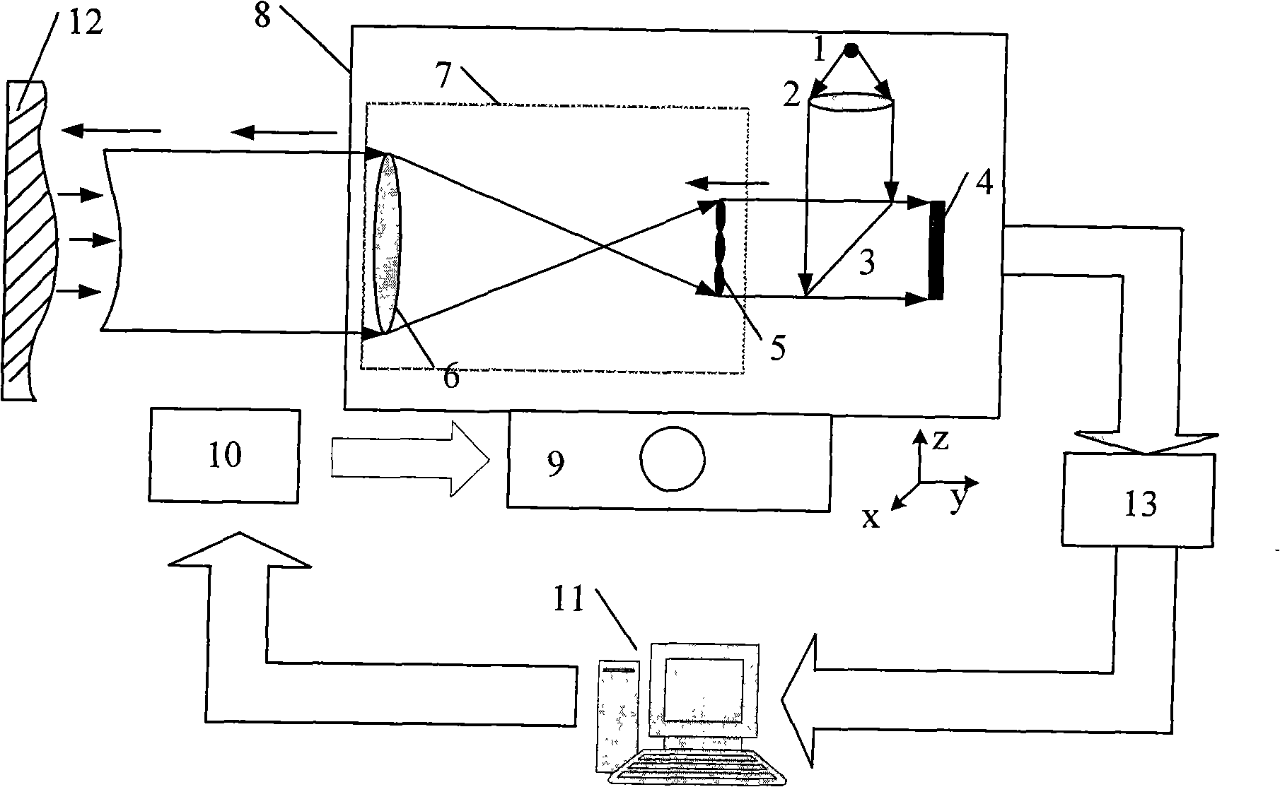
[0046] Such as figure 1 As shown, the splicing detection device based on the small-diameter circular Hartmann-Shack wavefront sensor of the present invention includes a Hartmann-Shack wavefront sensor 8, an x-z ​​two-dimensional electronically controlled translation stage 9, a stepper motor controller 10, and a computer 11, the mirror surface to be measured 12 and the data acquisition card 13; Hartmann-Shack wavefront sensor (8) detects a certain area of ​​the mirror surface to be measured (12) and forms light spot lattice at Hartmann-Shack wavefront sensor 8, by The data acquisition card 13 collects the above-mentioned spot data and transmits them to the computer 11 for storage; the computer 11 sends instructions to the stepper motor controller 10 to control the two-dimensional electronically controlled translation stage 9 to move along the...


PUM


Abstract

The invention discloses a splicing detection device of a circular Hartmann-Shack wave-front sensor based on a minor caliber. The device is characterized by comprising the Hartmann-Shack wave-front sensor, an x-z 2D electric control translation stage, a step motor controller, a computer, a mirror surface to be detected and a data acquisition card; the Hartmann-Shack wave-front sensor is positioned behind the mirror surface to be detected to detect the mirror surface to be detected, and a facula lattice is formed on the Hartmann-Shack wave-front sensor, and the data acquisition card acquires the facula data and transmits the data to the computer for storing; the computer sends an instruction to the step motor controller, and controls the 2D electric control translation stage to move along an x axis and a z axis to scan and detect the mirror surface to be detected; the data acquisition card sequentially acquires the facula data of a wavelet surface of each frame, and then a wave surface to be detected is obtained by a centroid algorithm, a splicing method and a restoration algorithm. The device and the method help improve a formula by ignoring a defocus error in theoretical analysis, eliminate a principle error of a translation error, improve splicing precision and lower computation complexity of solving splicing parameters.

Description

technical field [0001] The invention relates to the field of optical detection, in particular to a large-diameter optical system or a splicing detection system for components. Background technique [0002] Large-aperture optical components are being increasingly used in astronomical observation, space optics, remote sensing observation, laser fusion systems and other fields, and their processing and detection technology is a difficult and hot research topic at home and abroad. When using the conventional measurement method, it is very difficult to improve the measurement accuracy under the premise of considering the cost as the caliber increases. The use of small-caliber instruments to measure large-diameter optical components can better solve the contradiction between improving measurement accuracy and reducing equipment costs, and provides a new method for the detection of optical components. [0003] At present, a detection scheme of "sub-aperture splicing interferometer...

Claims


Application Information

Patent Timeline
IPC IPC(8): G01M11/00
Inventor 饶长辉郑翰清姜文汉饶学军杨金生樊志华
Owner INST OF OPTICS & ELECTRONICS - CHINESE ACAD OF SCI
Learn More