

Ultra-junction longitudinal bilateral diffusion metal oxide semiconductor tube
A vertical double-diffusion, semiconductor tube technology, used in semiconductor devices, electrical components, circuits, etc., can solve the problems of small drift layer thickness, no longer suitable for super junction structure devices, and high concentration in the drift region, and achieve an ideal off state, The effect of increasing the number and shortening the area
- Summary
- Abstract
- Description
- Claims
- Application Information
AI Technical Summary
Problems solved by technology
Method used
Image

Examples
Embodiment Construction
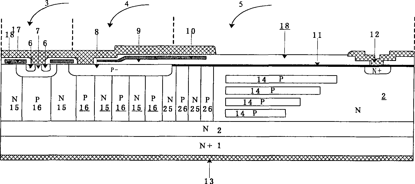
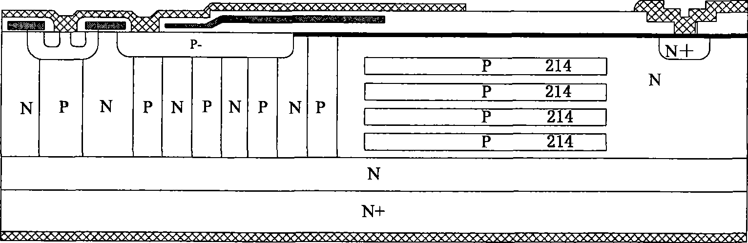
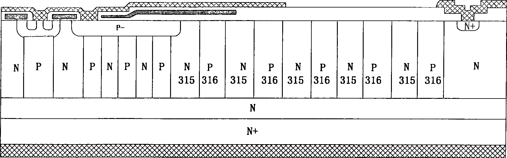
[0018] A super-junction vertical double-diffused metal oxide semiconductor tube, comprising: an N-type doped silicon substrate 1 serving as a drain region, an N-type doped silicon epitaxial layer 2, a primary cell region 3, and surrounding the primary cell region 13 The terminal region 5 and the transition region 4 between the original cell region 3 and the terminal region 5, the N-type doped silicon epitaxial layer 2 is arranged on the N-type doped silicon substrate 1, the original cell region 3 and the terminal region 5 is provided on the N-type doped silicon epitaxial layer 2, and the terminal region 5 of the transistor includes the first superjunction structure and the N-type silicon-doped semiconductor region 2 , wherein the first super junction structure includes N-type pillars 25 and P-type pillars 26, in the N-type silicon-doped semiconductor region 2 There are horizontal P-type columns 14 and high-concentration N-type regions in 12 , wherein the lengths of the transv...
PUM
 Abstract
Description
Claims
Application Information