

Photocarrier delay line
An optical carrier and delay line technology, applied in the field of delay lines, can solve problems such as limiting the application range of optical delay lines, and achieve the effect of light weight, small size, and continuously variable optical delay
- Summary
- Abstract
- Description
- Claims
- Application Information
AI Technical Summary
Problems solved by technology
Method used
Image

Examples
Embodiment Construction
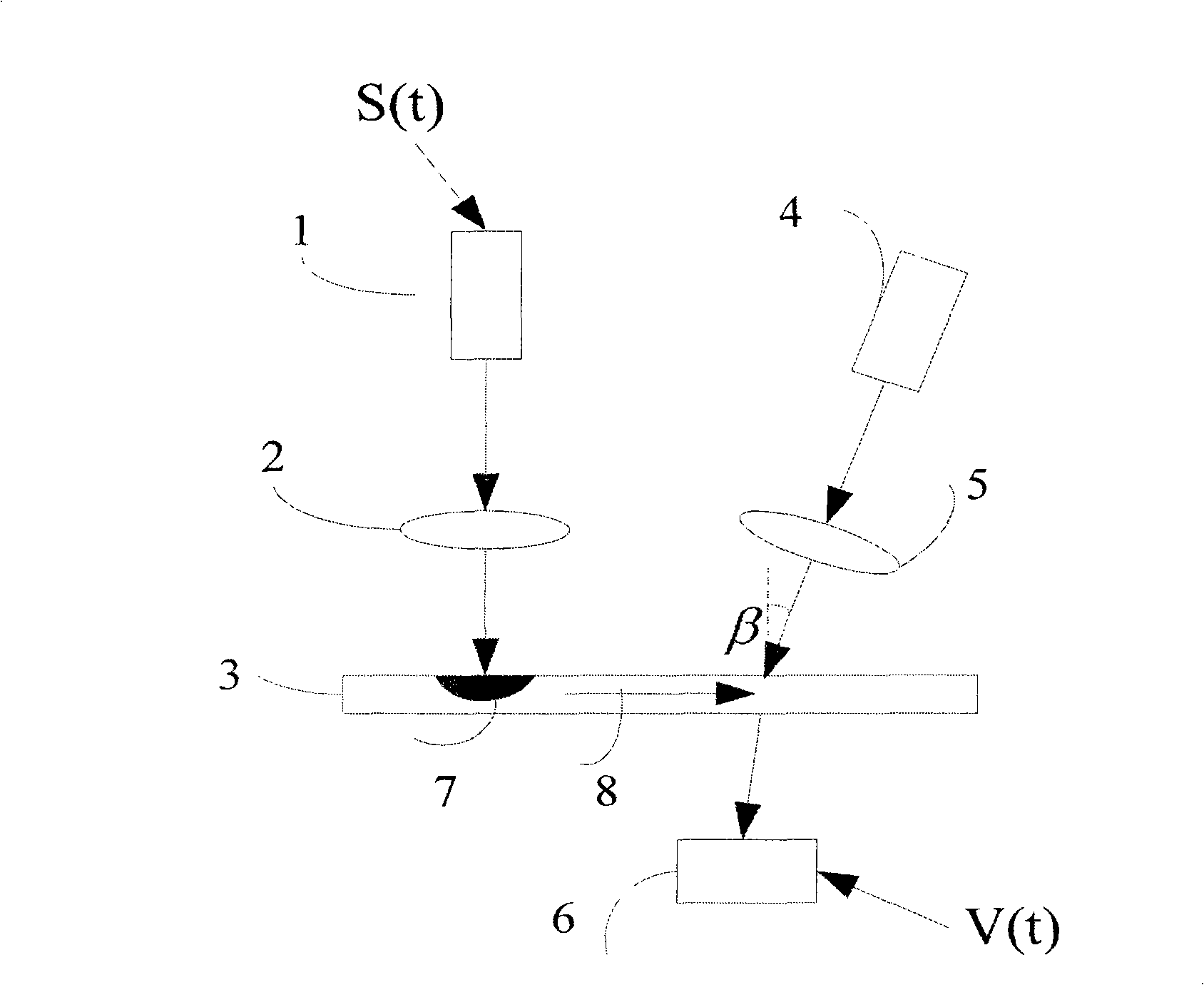
[0013] The present invention will be further described below in conjunction with accompanying drawing:
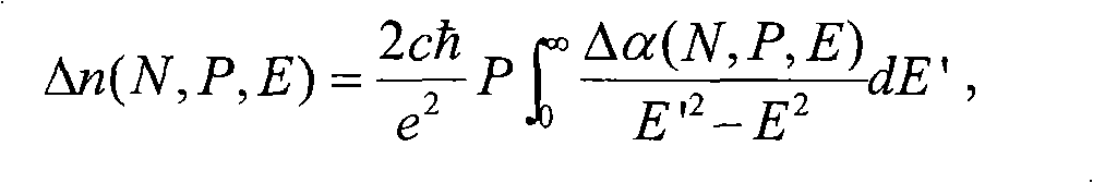
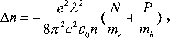
[0014] The basic principle of the present invention is as follows: a beam of excitation light (photon energy greater than the forbidden band width of semiconductor material) is incident on the surface of semiconductor material, and the material absorbs light energy and excites non-equilibrium carriers (electron-hole pairs), due to this Light injection causes a change in the non-equilibrium carrier concentration in the material, and the change in the carrier concentration will cause a change in the refractive index of the material. If the excitation light intensity is modulated by a radio frequency electrical signal, the modulated excitation light signal will be converted into a signal of refractive index change of the semiconductor material, and the refractive index change signal carries the information of the modulated excitation light signal. The non-equilibrium carriers ...
PUM
 Abstract
Description
Claims
Application Information