Off-axis alignment system and alignment method

An alignment system, off-axis technology, applied in the direction of optics, instruments, and pattern surface photolithography, can solve problems such as prolonging the alignment time, silicon wafer alignment errors, and affecting the productivity of lithography machines. Achieve the effect of improving the alignment process and ensuring accuracy

Active Publication Date: 2009-09-16
SHANGHAI MICRO ELECTRONICS EQUIP (GRP) CO LTD
View PDF1 Cites 4 Cited by
  • Summary
  • Abstract
  • Description
  • Claims
  • Application Information

AI Technical Summary

Problems solved by technology

[0004] This approach prolongs the entire alignment time and affects the productivity of the lithography machine
At the same time, when the silicon wafer marks are scanned, the off-axis optical axis cannot be accurately determined due to the vibration of the main frame, resulting in errors in the alignment of the silicon wafer

Method used


Image

  • Off-axis alignment system and alignment method
  • Off-axis alignment system and alignment method
  • Off-axis alignment system and alignment method

Examples


Embodiment Construction

[0039] In order to better understand the technical content of the present invention, specific embodiments are given and described as follows in conjunction with the accompanying drawings.

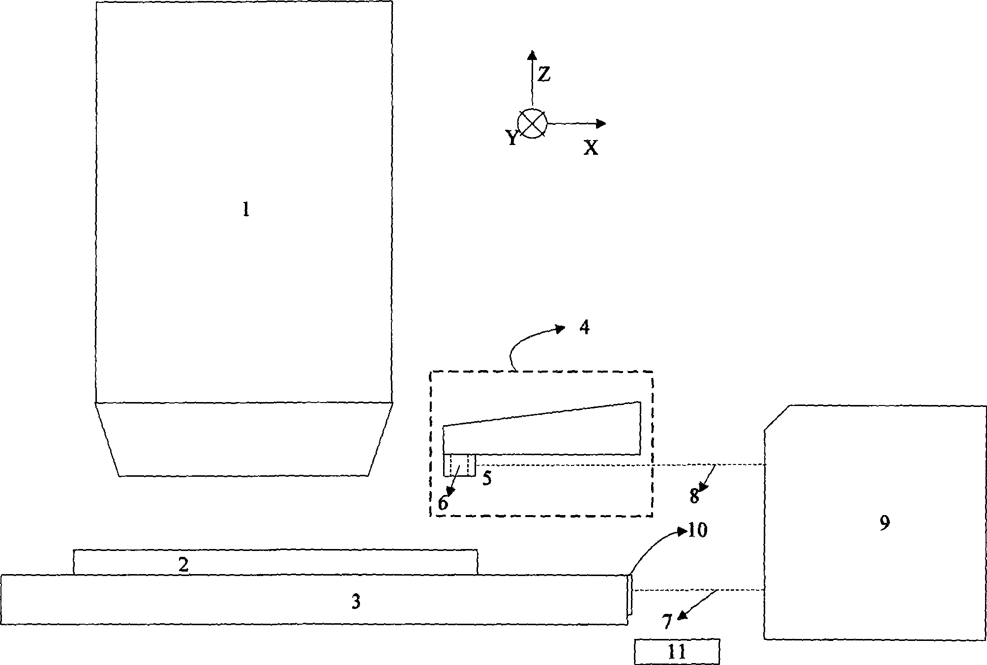
[0040] figure 1 Shown is a schematic structural diagram of a photolithographic apparatus with an off-axis alignment system in a preferred embodiment of the present invention.

[0041] The invention monitors the relative change of the off-axis optical axis at the alignment time in real time through the laser interferometer, and compensates to the scanning position of the silicon chip mark, establishes the relationship between the coordinates of the silicon chip and the workpiece table, and quickly realizes the alignment of the silicon chip. It includes three parts: the structure layout of the off-axis measurement system, the error correction of the measurement system, the compensation algorithm and the alignment algorithm of the off-axis system.

[0042] figure 1 The shown lithography appa...


PUM


Abstract

The invention provides an off-axis alignment system, which is used for lithographic equipment to ensure the position relationship of a silicon chip and a worktable. The off-axis alignment system comprises a laser interferometer, a zero position sensor, an off-axis optic system and a worktable; wherein, the laser interferometer is arranged along X direction and Y direction, and the laser interferometer is used for measuring the position of an off-axis optical axis and the worktable; the zero position sensor is arranged at the edge of the maximal motion range of the worktable and used for providing the initialization signal of the laser interferometer; the side of the off-axis optic system is provided with two off-axis reflecting surfaces respectively vertical to the X direction and the Y direction; and the side of the worktable is provided with two reflecting surfaces respectively vertical to the X direction and the Y direction, and the off-axis reflecting surfaces and the worktable reflecting surfaces are used for reflecting the measuring beams sent by the laser interferometer. The laser interferometer is added in the off-axis alignment system, so that the excursion of the off-axis plain shaft in the alignment system can be detected in real time and the alignment precision of the silicon chip can be ensured.

Description

technical field [0001] The invention relates to a processing device for silicon wafer alignment, and in particular to an off-axis alignment system, and an alignment method of the off-axis alignment system. Background technique [0002] The purpose of the projection scanning lithography machine is to clearly and correctly image the pattern on the mask on the silicon wafer coated with photoresist. The function of the off-axis alignment system in the lithography machine is to determine the position of the silicon wafer during exposure. [0003] In US Pat. No. 7,332,732B2 describing the layout and measurement method of the off-axis system, a reference plate with off-axis marks is fixed on the lower right side of the workpiece table. First, the relative position of the off-axis optical axis in the workpiece table is captured by scanning the off-axis marks on the reference plate of the workpiece table, and then the relationship between the silicon wafer and the workpiece table is ...

Claims


Application Information

Patent Timeline
Patent Type & Authority Applications(China)
IPC IPC(8): G03F9/00G03F7/20
Inventor 方立孙刚
Owner SHANGHAI MICRO ELECTRONICS EQUIP (GRP) CO LTD
Why Eureka
Try Eureka