

Adhesive tape and semiconductor device using the same
A semiconductor and adhesive tape technology, applied in the field of adhesive tape, can solve the problems of difficulty in ensuring the electrical connection reliability of semiconductor chips, resin ion migration resistance, inability to achieve high density of semiconductor integrated circuits, etc. Achieving the effect of reducing weight and improving wettability
- Summary
- Abstract
- Description
- Claims
- Application Information
AI Technical Summary
Problems solved by technology
Method used
Image

Examples
no. 1 approach
[0079] First, the adhesive tape according to the first embodiment of the present invention will be specifically described.
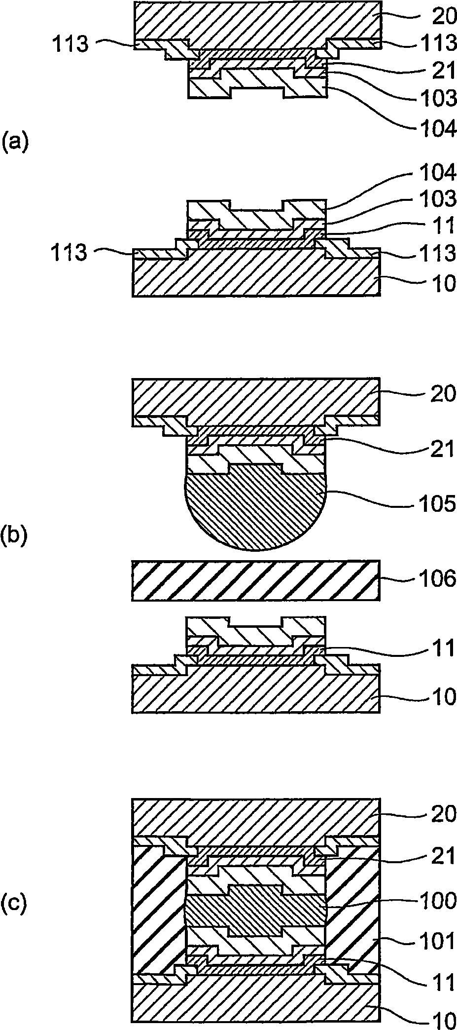
[0080] The adhesive tape according to the first embodiment of the present invention is an adhesive tape containing (A) a film-forming resin, (B) a curable resin, and (C) a curing agent having flux activity in a predetermined compounding ratio. The adhesive tape according to the first embodiment of the present invention is particularly suitable for use when electrically connecting semiconductor chips by flip-chip in a stacked-chip semiconductor device in which semiconductor chips are flip-chip mounted. . The adhesive tape according to this embodiment is thermally fused by being interposed between semiconductor chips facing each other, thereby removing the oxide film of the solder component constituting the solder bump formed on the facing surface side of at least one semiconductor chip, Thereby, the wettability of the solder component is improved, the so...
no. 2 approach
[0157] Next, an adhesive tape according to a second embodiment of the present invention will be described.
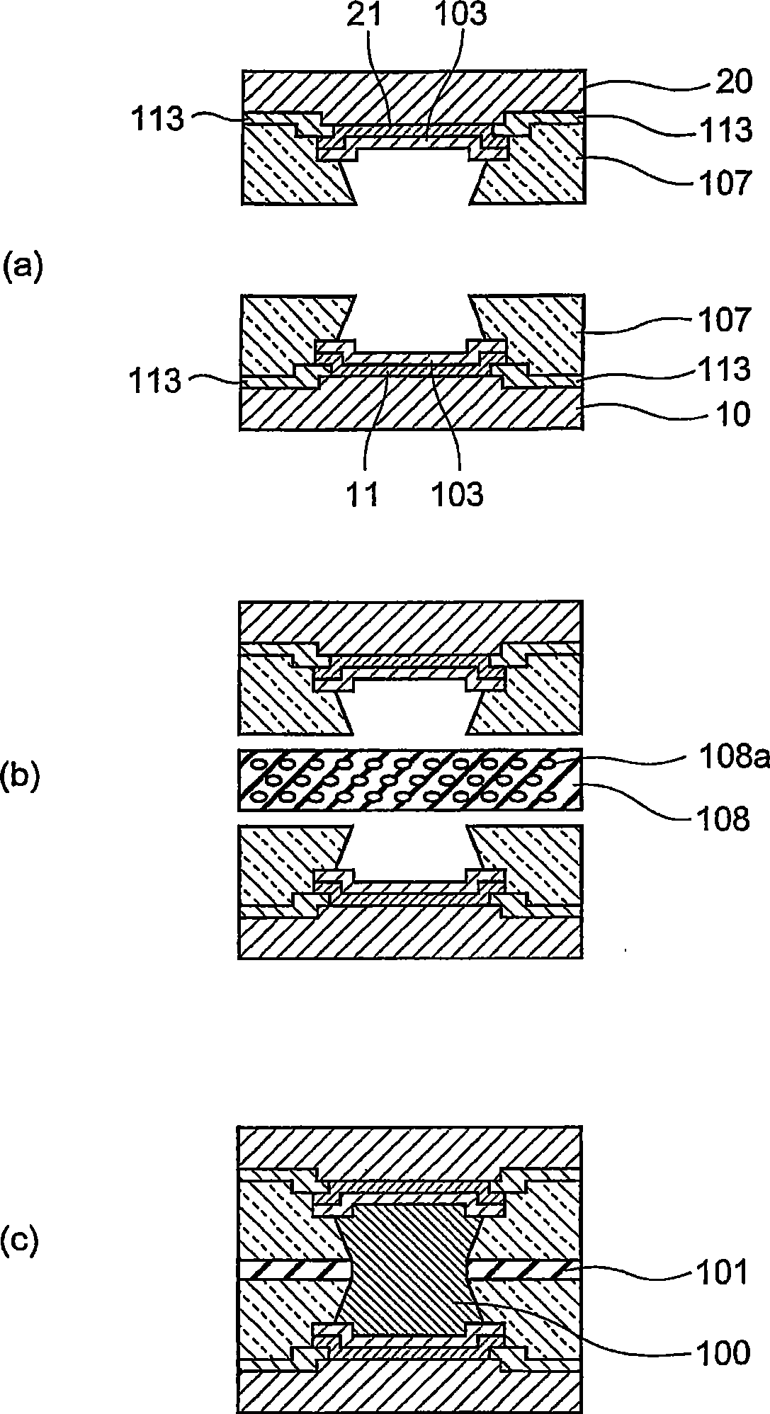
[0158] The adhesive tape according to the second embodiment of the present invention contains (E) solder powder in a predetermined compounding ratio in addition to (A) a film-forming resin, (B) a curable resin, and (C) a curing agent having flux activity. . The adhesive tape according to the second embodiment of the present invention is particularly suitable for utilizing the self-alignment (Self- Alignment) is used for electrical connection between semiconductor chips. The adhesive tape of this embodiment is thermally fused by being interposed between opposing semiconductor chips, and the solder powder contained in the adhesive tape aggregates between opposing internal electrodes to promote the formation of a solder region. , and the resin component is filled in the gap between the semiconductor chips to promote the formation of the insulating region. By curing the r...
Embodiment approach
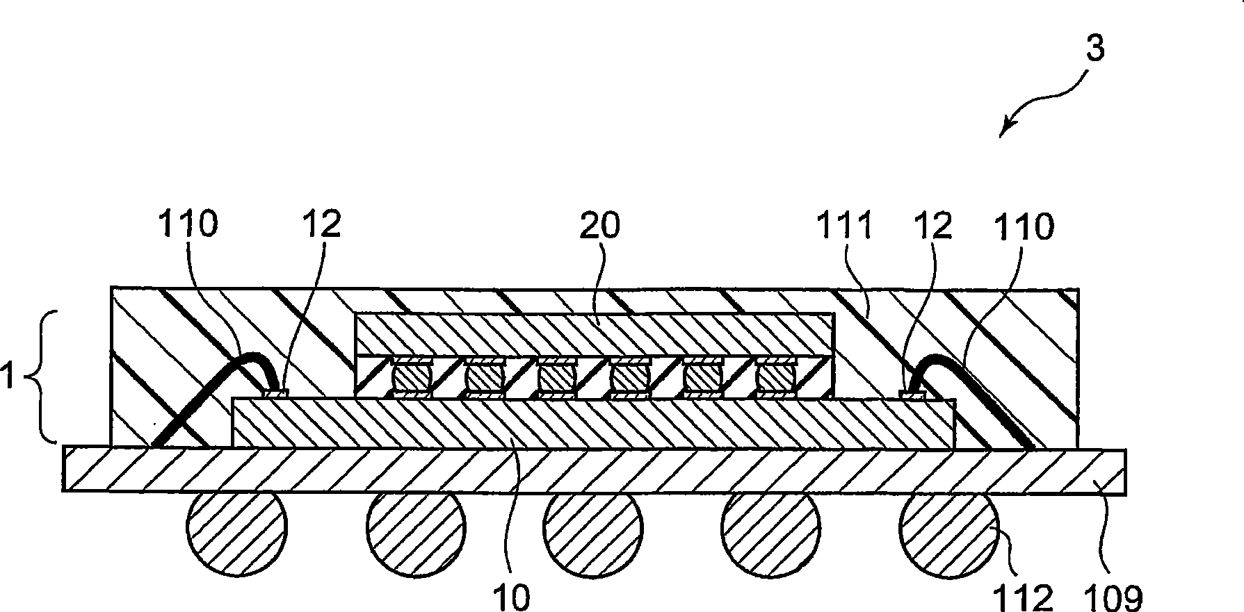
[0177]The semiconductor device of the present invention is a stacked chip type semiconductor device in which semiconductor chips are electrically connected to each other using the adhesive tape of the present invention. As one embodiment of the present invention, for example, a semiconductor device includes a first semiconductor chip and a second semiconductor chip, and includes a circuit surface of the first semiconductor chip and a circuit surface of the second semiconductor chip facing each other. A laminated chip-type semiconductor electronic component placed and arranged, wherein the first semiconductor chip and the second semiconductor chip are bonded with the adhesive tape of the present invention. In addition, another embodiment of the present invention includes a semiconductor device including a plurality of third semiconductor chips further stacked on the side opposite to the circuit side of the second semiconductor chip in the semiconductor device. A layer-stacked s...
PUM
| Property | Measurement | Unit |
|---|---|---|
| diameter | aaaaa | aaaaa |
| thickness | aaaaa | aaaaa |
| softening point | aaaaa | aaaaa |
Abstract
Description
Claims
Application Information