Substrate for an organic light-emitting device, use and process for manufacturing this substrate, and organic light-emitting device

A technology for organic light-emitting devices and substrates, which can be used in electroluminescent light sources, lighting devices, optics, etc., and can solve the problems of increased surface roughness and decreased transparency.

Inactive Publication Date: 2009-09-16
SAINT-GOBAIN GLASS FRANCE
View PDF11 Cites 28 Cited by
  • Summary
  • Abstract
  • Description
  • Claims
  • Application Information

AI Technical Summary

Problems solved by technology

Unless the layer thickness is increased to greater than 150 nm, the sheet resistance remains relatively high ( leve

Method used


Image

  • Substrate for an organic light-emitting device, use and process for manufacturing this substrate, and organic light-emitting device
  • Substrate for an organic light-emitting device, use and process for manufacturing this substrate, and organic light-emitting device
  • Substrate for an organic light-emitting device, use and process for manufacturing this substrate, and organic light-emitting device

Examples


Embodiment 5

[0249] Example 5 constructs an optimized example compared to the relative-example, ie, Example 6, which has a TCO (ITO) electrode. It can be seen from the above table that the sheet resistance, roughness, performance and life characteristics of Example 5 are better than that of Example 6.

[0250] In Example 7, the coated substrate can be used as a transparent / reflective electrode because the T of the coated substrate L / R L The ratio is 0.2, which is between 0.1-0.7. In addition, the light transmission of the coated substrate is less than 50%, therefore, it cannot be used to prepare transparent electrodes, but it can be used to prepare reflective electrodes because of its light reflection is greater than 70%.

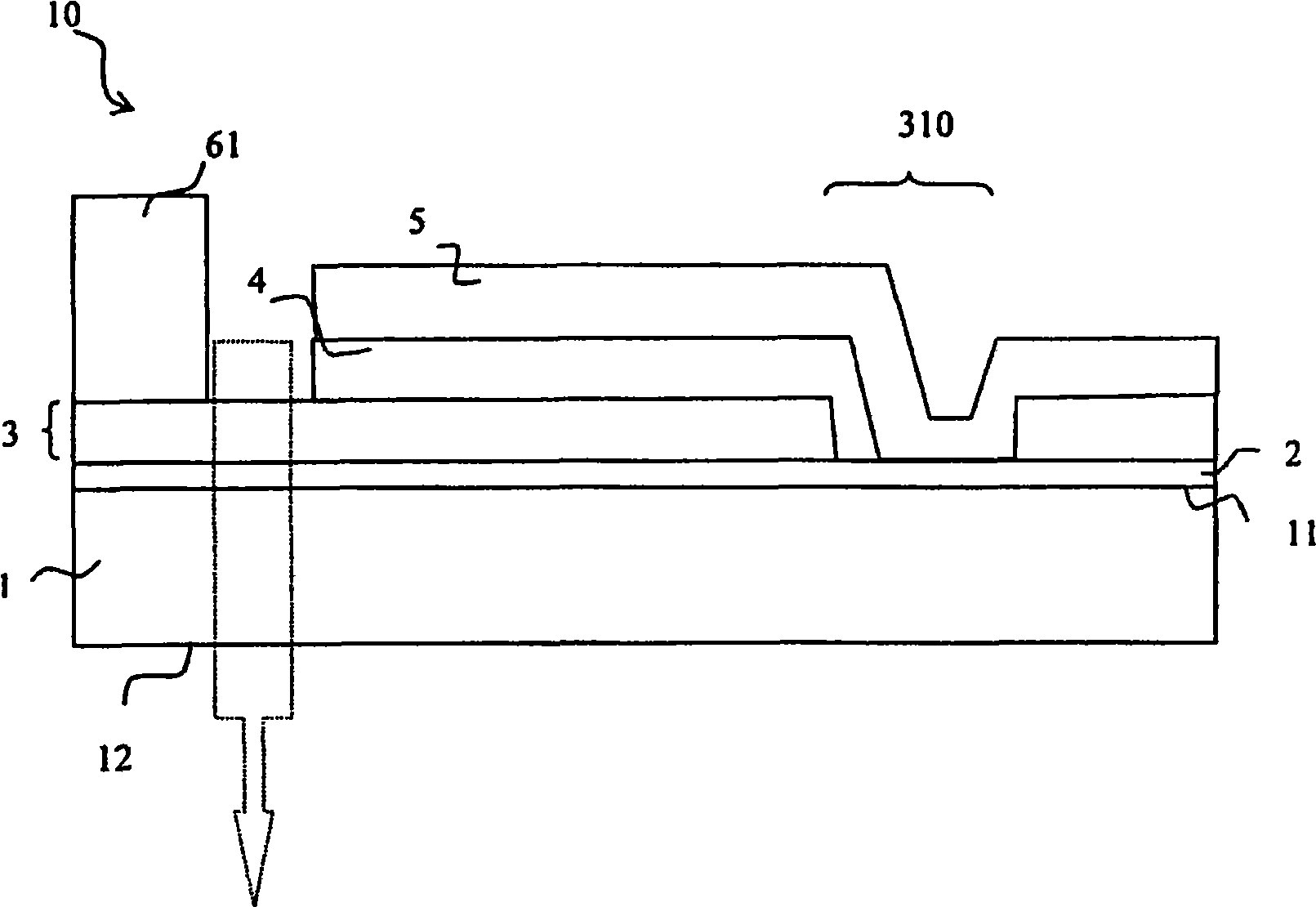
[0251] The first electrode may or may substantially be a reflective electrode.

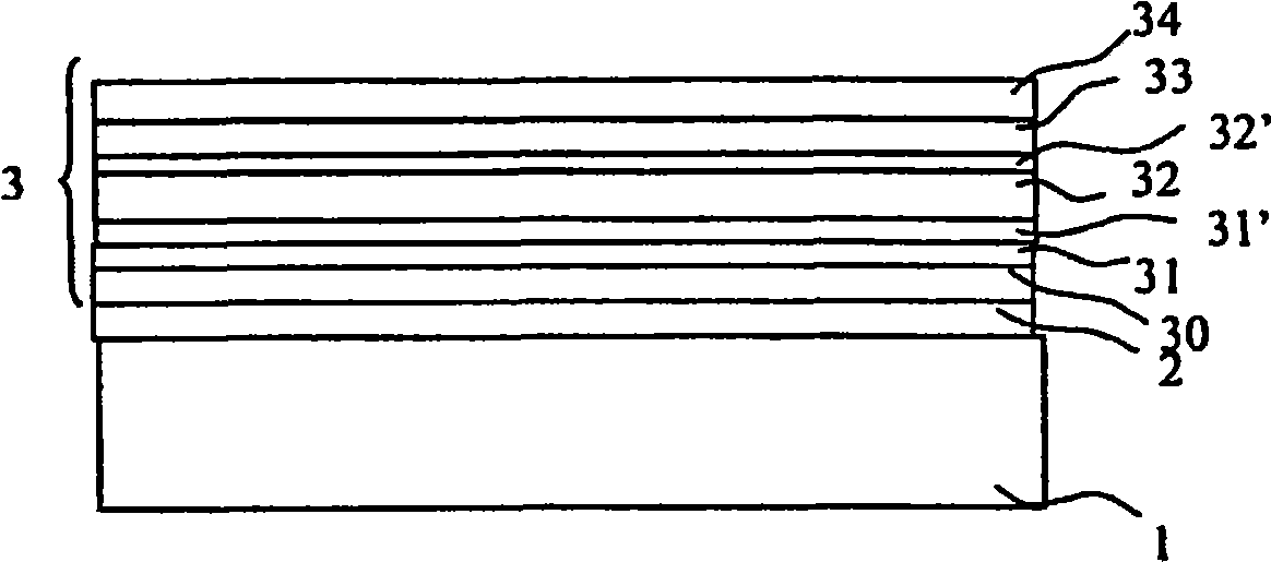
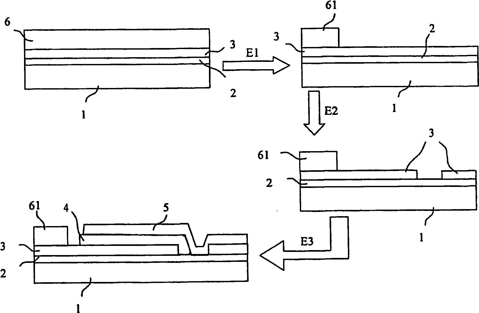
[0252] The bottom electrode 3 extends along one side of the substrate 1 . Thus, immediately above the edge of the cover layer 34 there is a first metallic current source strip 61, pref...


PUM

PropertyMeasurementUnit
Thicknessaaaaaaaaaa
Roughnessaaaaaaaaaa
Thicknessaaaaaaaaaa

Abstract

The invention relates to a substrate (1) for an organic light-emitting device (10), especially a transparent glass substrate, comprising, on a first main face (11), a lower electrode coating (3), the electrode coating (3) consisting of a thin-film multilayer comprising, in succession, at least: a contact layer (31) based on a metal oxide and/or metal nitride; a metallic functional layer (32) having an intrinsic electrical conductivity property; and an overlayer (34) based on a metal oxide and/or metal nitride, especially for matching the work function of said electrode coating, said substrate including a bottom layer (2), said bottom layer (2) covering said main face (11).

Description

technical field [0001] The subject of the invention is a multilayer electrode, its acid etching and an organic light-emitting device comprising it. Background technique [0002] Known organic light-emitting systems or OLEDs comprise organic electroluminescent materials or multilayer coatings of organic electroluminescent materials, which are charged via electrodes, usually in the form of two conductive layers on either side of them. [0003] These conductive layers generally comprise layers based on indium oxide, usually tin-doped indium oxide, the abbreviation ITO being more common for tin-doped indium oxide. The ITO layer has been studied particularly intensively. They can be easily deposited by magnetron sputtering, using either oxide targets (non-reactive sputtering) or targets based on indium and tin (reactive sputtering in the presence of oxygen-type oxidants), and Their thickness is about 100-150 nm. However, such ITO layers have a number of disadvantages. First, ...

Claims


Application Information

Patent Timeline
IPC IPC(8): H05B33/26H01L51/52G02F1/1343H01J1/30
CPCH01J1/30H01L51/5203H01L51/5237H05B33/26G02F1/13439H10K59/86H10K50/816H10K50/805
Inventor S·恰库罗夫H·热拉尔丹P·雷乌特勒D·茹斯E·马特曼恩P·内尔
Owner SAINT-GOBAIN GLASS FRANCE
Why Eureka
Try Eureka