

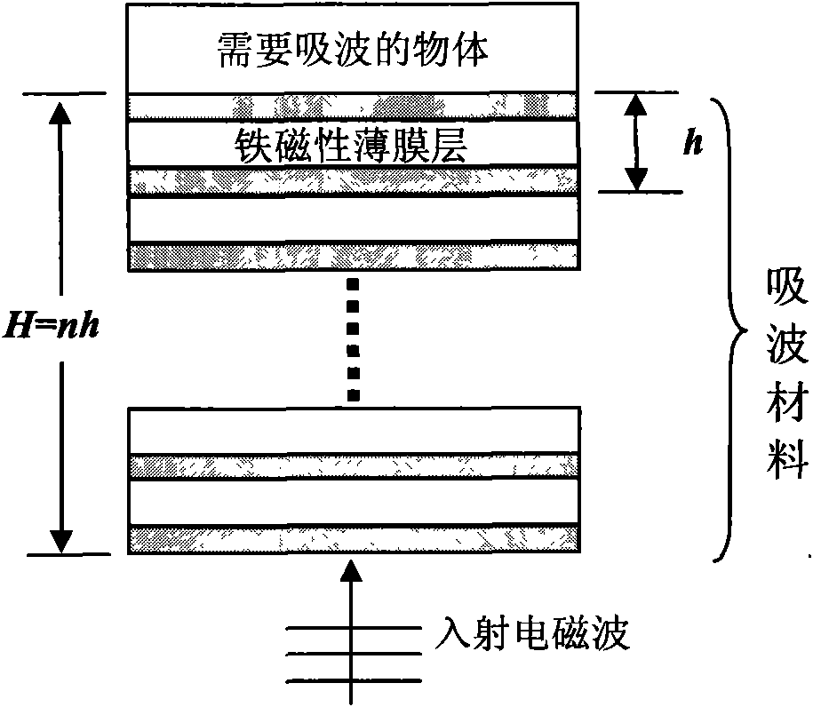
Ferromagnetic thin-film wave absorbing material with periodic structure
A technology of ferromagnetic film and wave-absorbing materials, which is applied to the parts, shielding, instruments, etc. of instruments to achieve the effect of convenient operation, good wave-absorbing performance, and simple structure improvement
- Summary
- Abstract
- Description
- Claims
- Application Information
AI Technical Summary
Problems solved by technology
Method used
Image

Examples
Embodiment 1
[0032] Material:
[0033] The dielectric layer is SiO 2 Or polyethylene terephthalate d=2~10nm
[0034] Ferromagnetic thin film layer d=0.25μm
[0035] Using a radio frequency magnetron sputtering device, in an Ar gas environment, Fe is sputtered and deposited on the dielectric layer through magnetic orientation, and then the ferromagnetic thin film layer and SiO 2 Or polyethylene terephthalate dielectric films are alternately arranged to form a laminated multilayer film. Due to SiO 2 , Si, polyester, especially polyethylene terephthalate and other materials have relatively stable chemical properties, so they are often used as dielectric materials. Simultaneously, the function of the medium layer in the present invention is to separate the two ferromagnetic film layers, and the thickness of the medium layer can be made as small as possible, so as to reduce the total thickness of the magnetic film. Within the precision range of commonly used devices in this field, the thic...
Embodiment 2
[0037]Material:
[0038] The dielectric layer is SiO 2 Or polyethylene terephthalate dielectric layer thickness: d = 2 ~ 10nm
[0039] Ferromagnetic thin film layer Film thickness: d=0.3μm
[0040] Ar+N 2 mixed gas N 2 Gas concentration can be controlled
[0041] Adopt radio frequency magnetron sputtering device, the present invention has used the Lab18 type magnetron sputtering equipment of U.S. Lesker company, by Ar+N 2 Sputtering deposition of Fe on SiO in a mixed gas 2 Or polyethylene terephthalate film, Ar gas and N in this embodiment 2 The gas ratio is controlled at 24:6. In the present invention, generally Ar and N 2 N in mixed gas 2 The volume of the gas is controlled at 20% to 50%, the pressure of the mixed gas is 0.2Pa, and the ambient temperature is 160°C to 250°C, which can ensure that the mass ratio of the final N element in the ferromagnetic film layer is not greater than 10%. It has a slight effect on the saturation magnetization of ferromagnetic thin ...
PUM
| Property | Measurement | Unit |
|---|---|---|
| Thickness | aaaaa | aaaaa |
| Thickness | aaaaa | aaaaa |
| Thickness | aaaaa | aaaaa |
Abstract
Description
Claims
Application Information