
Semiconductor package structure having movable gain variation on circumsphere point

A technology of gain change and circumscribed ball, which is applied in the direction of semiconductor devices, semiconductor/solid-state device parts, electric solid-state devices, etc., can solve problems such as fracture and ball drop, substrate warping, prone to overflowing or climbing glue, etc., to achieve The effect of reducing stress and avoiding fracture

Inactive Publication Date: 2009-10-07
POWERTECH TECHNOLOGY
View PDF0 Cites 2 Cited by
  • Summary
  • Abstract
  • Description
  • Claims
  • Application Information

AI Technical Summary

Problems solved by technology

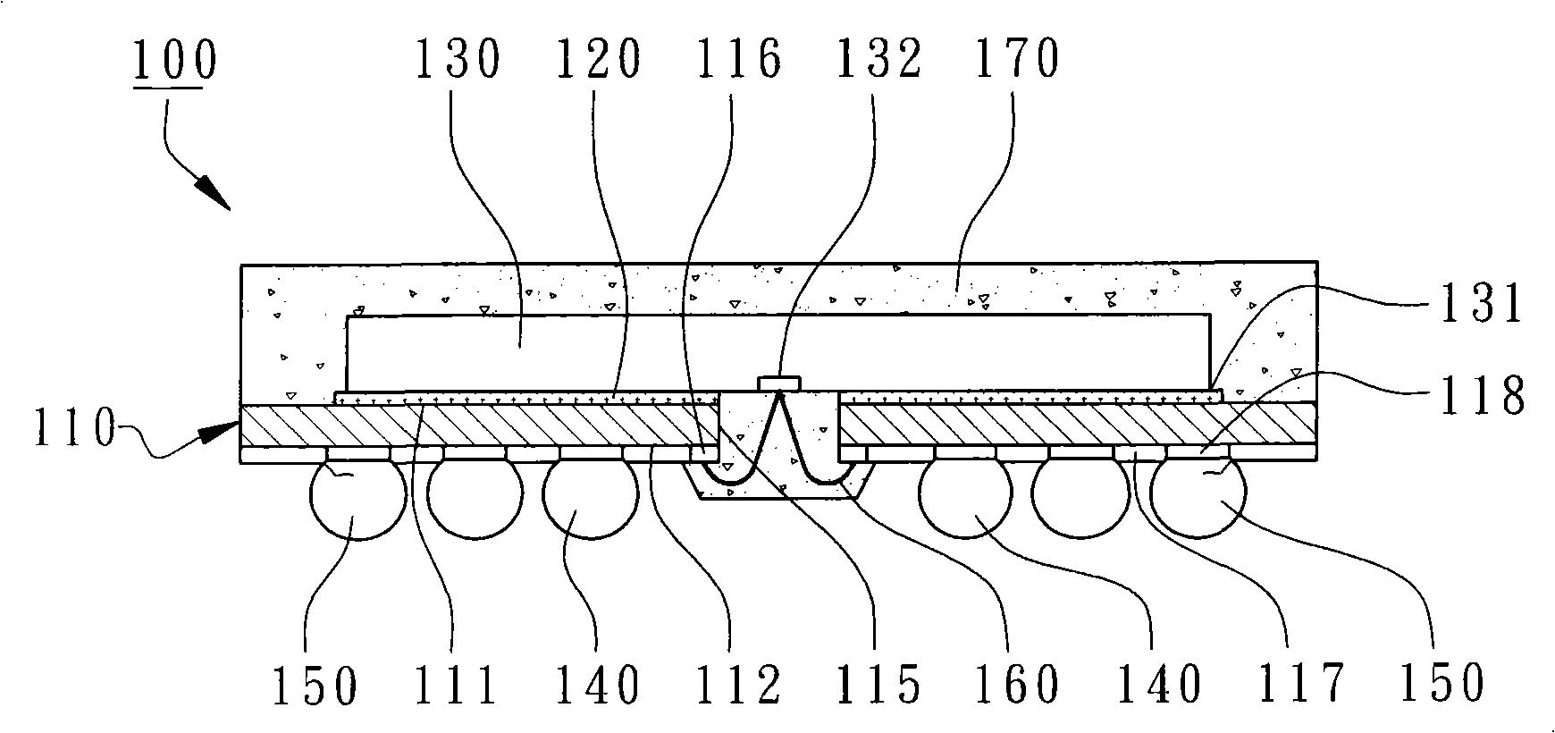
[0006] However, in the curing of the above-mentioned die-bonding adhesive material 120, the curing of the encapsulant 170, the first row of circumscribed ball points 140 and the second row of circumscribed The reflow welding of ball point 150 or the follow-up thermal cycle test and actual product calculation will have heat treatment. The difference in thermal expansion coefficient between materials will cause thermal stress, or impact stress will be generated in the drop test. These stresses will be applied These 2nd row outer contact points 150 cause breakage and ball drop problems, which affect the quality of electrical connections
In addition, the substrate 110 is prone to warpage
Parts of the first row of outer ball pads 140 or the second row of outer ball pads 150 adjacent to the side corners 131 of the chip 130 also have problems with breakage and ball drop
In addition, during the heating and pressure process of die bonding, the die bonding adhesive material 120 has fluidity and is prone to overflow or creep.

Method used


Image

  • Semiconductor package structure having movable gain variation on circumsphere point
  • Semiconductor package structure having movable gain variation on circumsphere point
  • Semiconductor package structure having movable gain variation on circumsphere point

Examples


no. 1 Embodiment

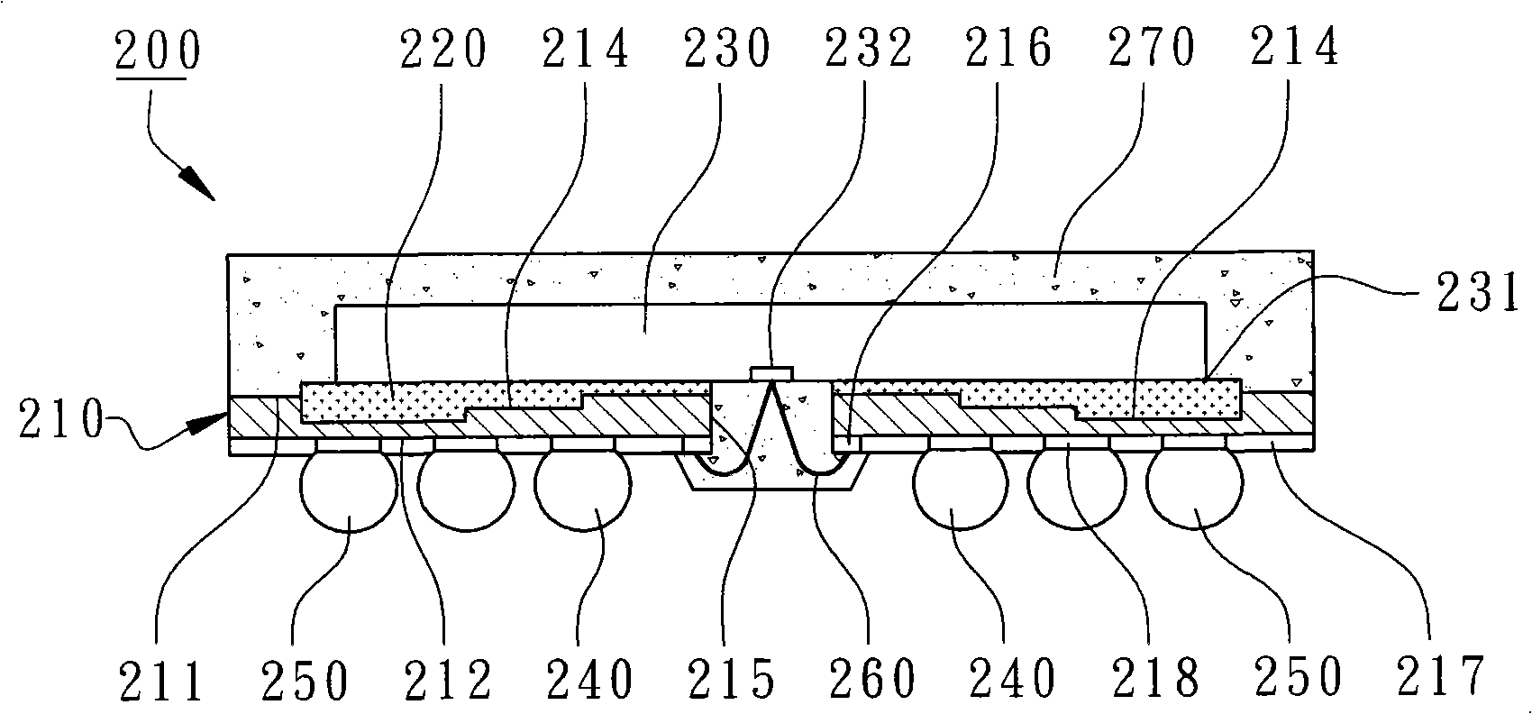
[0073] According to the first embodiment of the present invention, it discloses a semiconductor package structure with a circumscribed ball having movable gain variation.

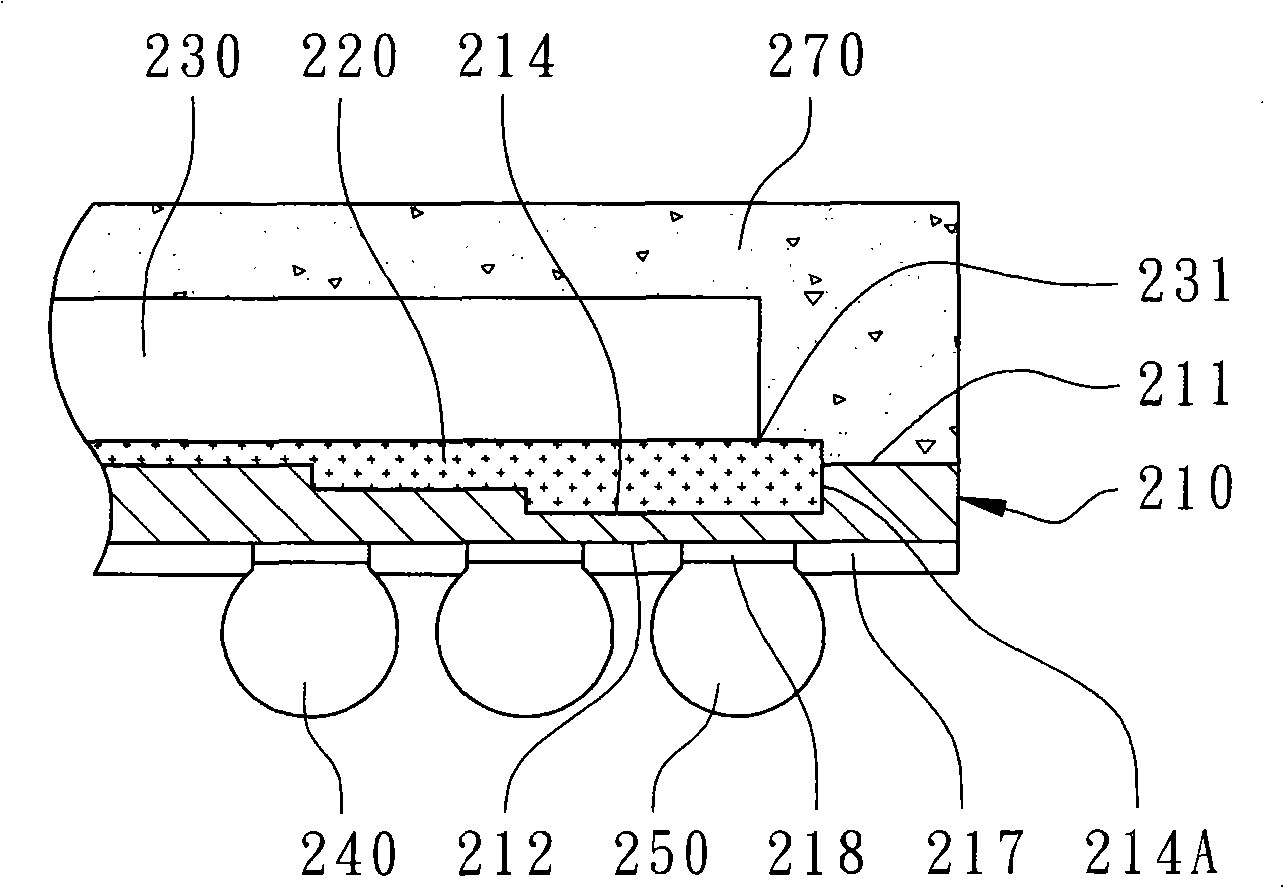
[0074] Such as figure 2 and image 3 As shown, the semiconductor package structure 200 mainly includes a substrate 210 , a die-bonding adhesive 220 , a chip 230 , two or more first rows of outer balls 240 and two or more second rows of outer balls 250 .

[0075] The substrate 210 has a package surface 211, an exposed surface 212 and a through hole 215, wherein the package surface 211 includes a die bonding area 213, such as Figure 4 As shown, the size of the die attach 213 may be approximately equal to the size of the chip 230 .

[0076] Wherein, these second rows of external ball points 250 are linearly arranged in a manner parallel to the center line of the die bonding area 213, and these second row of external ball points 250 are farther away from the center line relative to these first row of extern...

no. 2 Embodiment

[0088] The second specific embodiment of the present invention discloses another semiconductor package structure with a movable gain change at the external ball point, which can use a back-to-back double-chip stacked window ball grid array package product (back-to-back DDP WBGA), mainly The components are substantially the same as those of the first embodiment, so the same reference numerals are used, see Figure 6 As shown, for example, a substrate 210 , a die-bonding adhesive 220 , a first chip 230 , a first row of outer ball pads 240 and a second row of outer ball pads 250 . The semiconductor package structure may further include a second chip 280 stacked on the backside of the chip 230 back to back. But without limitation, more chips can be stacked on top, such as three, four or more, to form a multi-chip stacked package structure, which can improve operating efficiency. Specifically, the active surface of the second chip 280 has two or more second bonding pads 281, and c...

no. 3 Embodiment

[0090] The third embodiment of the present invention discloses another semiconductor package structure in which the circumscribing ball has movable gain variation. see Figure 7 As shown, the semiconductor package structure 300 mainly includes a substrate 310 , a die-bonding adhesive 320 , a chip 330 , two or more first rows of outer balls 340 and two or more second rows of outer balls 350 . The substrate 310 has a packaging surface 311 and an exposed surface 312, wherein the packaging surface 311 includes a die-bonding region 313, such as Figure 8 As shown, the size of the die-bonding region 313 may be approximately equal to the size of the chip 330 . The exposed surface 312 of the substrate 310 may be formed with a solder mask layer 317, which is an insulating material, to form an electrically insulating layer covering the conductive traces, but exposing two or more external pads. 318, so that the first row of outer ball points 340 and the second row of outer ball points ...


PUM


Abstract

The invention discloses a semiconductor package structure having movable gain variation on a circumsphere point, comprising a substrate, crystal bonded plastic, a chip, two or more first rows of circumsphere points and two or more second rows of circumsphere points. The substrate has a package surface and an exposing surface, wherein the package surface has a crystal bonded area; the crystal bonded plastic is formed on the package surface of the substrate; the chip is aligned in the crystal bonded area and arranged on the package surface of the substrate by means of the crystal bonded plastic; the two or more first rows of circumsphere points are arranged on the exposing surface of the substrate; and the two or more second rows of circumsphere points are arranged on the exposing surface of the substrate, and are away from the central line of the crystal bonded area relative to the first rows of circumsphere points, wherein the substrate is also provided with at least one cascade groove formed on the package surface so that the thickness of the substrate in the cascade groove is thinned in a cascade shape towards the direction of the central line of the crystal bonded area, and the crystal bonded plastic is filled in the cascade groove. The cascade groove provides an accommodating space for the crystal bonded plastic so as to reduce overflow pollution.

Description

technical field [0001] The present invention relates to a semiconductor device using semiconductor packaging technology, in particular to a semiconductor package structure in which circumscribing balls have movable gain changes. Background technique [0002] Currently, semiconductor package structures have various package types depending on the integrated circuits of semiconductor chips packaged inside. The so-called ball grid array (BGA, ball grid array) packaging structure is provided with two or more external ball points (generally referred to as solder balls or solder reflow) on the bottom surface of the product. ball). The external ball points should be formed on the same bonding plane and have an appropriate and sufficient number as the I / O connecting terminal of the semiconductor package structure, so as to form an electrical connection with the external printed circuit board during operation relationship to meet the needs of high-density surface bonding. Typically...

Claims


Application Information

Patent Timeline
IPC IPC(8): H01L23/488H01L23/13H01L23/31H01L25/00
CPCH01L2924/1515H01L2924/15311H01L2224/73265H01L2224/83385H01L2224/48227H01L2224/4824H01L2924/3025H01L2225/06558H01L2224/32225H01L2224/73215H01L2924/181
Inventor 范文正
Owner POWERTECH TECHNOLOGY
Learn More