Packaging method of improving antistatic capability of integrated circuit chip
A technology of integrated circuits and packaging methods, applied in circuits, electrical components, electrical solid devices, etc., to achieve the effect of reducing voltage drop
- Summary
- Abstract
- Description
- Claims
- Application Information
AI Technical Summary
Problems solved by technology
Method used
Image
Examples
Embodiment Construction
[0073] In order to make the object, technical solution and advantages of the present invention clearer, the present invention will be described in further detail below in conjunction with specific embodiments and with reference to the accompanying drawings.
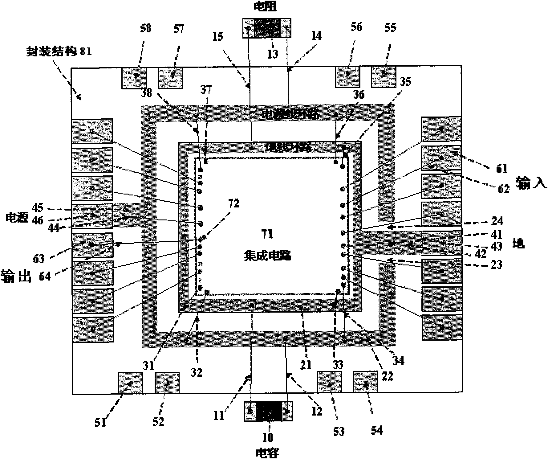
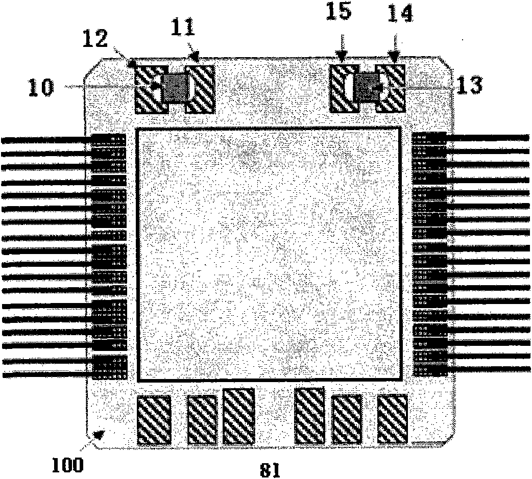
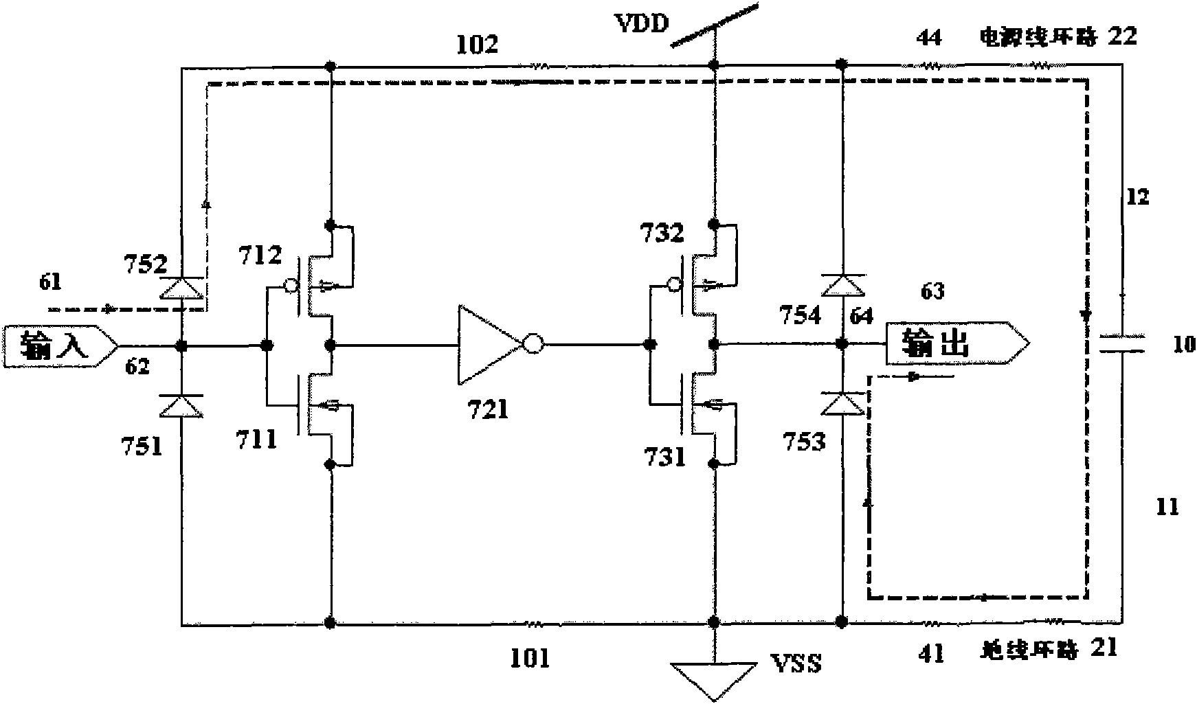
[0074] The packaging method for improving the antistatic ability of the integrated circuit chip provided by the present invention adopts the method of adding a capacitor between VDD and VSS to reduce the ESD voltage to a very low level and add it to the integrated circuit, and connect the two ends of the capacitor in parallel The resistor effectively discharges the charge stored on the capacitor, which can ensure that the internal circuit of the chip will not be damaged when it withstands multiple ESD voltages with an interval of 1 second, effectively ensuring that the chip has good ESD protection after packaging performance.
[0075] figure 1 It is an exemplary packaging structure with ESD capacitor protection of a sing...
PUM
| Property | Measurement | Unit |
|---|---|---|
| Thickness | aaaaa | aaaaa |
| Width | aaaaa | aaaaa |
| Capacitance | aaaaa | aaaaa |
Abstract
Description
Claims
Application Information


