Transparent conducting film and writing-resistance high-penetrability resistance-type touching control panel using same

A transparent conductive film, touch panel technology, applied in conductive layers on insulating carriers, electrical digital data processing, input/output process of data processing, etc. , to achieve the effect of improving optical transmittance, improving writing resistance, and increasing structural strength

Active Publication Date: 2009-10-28
USHINE PHOTONICS CORP
View PDF0 Cites 19 Cited by
  • Summary
  • Abstract
  • Description
  • Claims
  • Application Information

AI Technical Summary

Problems solved by technology

[0010] The technical problem to be solved by the present invention is to provide a transparent conductive film with write resistance and high optical transmittance and a resistive touch panel using the transparent conductive film, so as to solve the problem of transparent conductive film and touch control in the prior art. The panel has the problems of not being resistant to writing and poor optical transmission characteristics

Method used


Image

  • Transparent conducting film and writing-resistance high-penetrability resistance-type touching control panel using same
  • Transparent conducting film and writing-resistance high-penetrability resistance-type touching control panel using same
  • Transparent conducting film and writing-resistance high-penetrability resistance-type touching control panel using same

Examples


Embodiment Construction

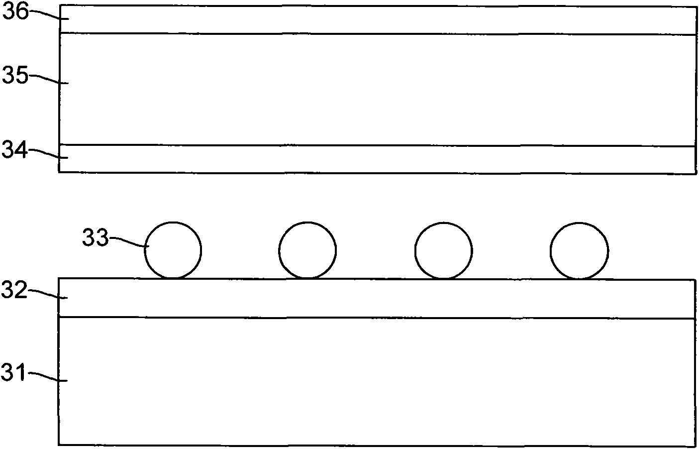
[0039] The design of the conductive film with high optical transmittance is described below. Generally, the transparent conductive film used in the touch panel is composed of a thin film layer of PET and ITO plated on it, that is, in figure 1 Among them, the second base material is PET (polyethylene terephthalate, Polyethylene Terephthalate, PET), and the second conductive layer is an ITO layer, the design of this kind of transparent conductive film, its anti-reflection effect is not good, even By adjusting the thickness of the ITO film layer, the room for improving the overall optical transmittance is very limited. However, by means of optical design, the multilayer film structure can be designed on the existing ITO-PET structure, so that the optical properties can be greatly improved. For example, if image 3 As shown, first on the PET substrate (as the second substrate 21 of the accompanying drawing), a high-refractive-index material (ie, the first dielectric layer 18, who...


PUM

PropertyMeasurementUnit
thicknessaaaaaaaaaa
thicknessaaaaaaaaaa
thicknessaaaaaaaaaa

Abstract

The invention discloses a transparent conducting film and a writing-resistance high-penetrability resistance-type touching control panel using the same. The transparent conducting film comprises a first substrate material, a first hardening treatment layer which is arranged on the first substrate material, a colloid which is used for bonding one side of an unhardened layer of the first substrate material and a second substrate material, a first dielectric layer which is arranged on the other side of the second substrate material and has an optical refractive index of n1, a second dielectric layer which is arranged under the first dielectric layer and has an optical refractive index of n2, and a first conducting layer which is arranged under the second dielectric layer and has a refractive index of n3, wherein the refractive indexes of the film layer materials satisfy the equation that n3 is more than n2 and less than or equal to n1 as well as a film stack structure of substrate-high refractive index-low refractive index-high refractive index; and the film layer materials can form an antireflection film layer to improve the optical permeability of the transparent conducting film in a range of visible light. The transparent conducting film adopting a multilayer structure allows the conducting layer in the transparent conducting film to increase the allowable external stress bearing capacity effectively and improves the structural strength and writing resistance of the touching control panel.

Description

technical field [0001] The invention relates to the application of a transparent conductive film in a resistive touch panel, in particular to a write-resistant conductive film with high optical penetration and a resistive touch panel using the transparent conductive film. Background technique [0002] The transparent conductive film is one of the main components of the resistive touch panel. A resistive-type touch panel mainly calculates the position of a touch point by measuring and comparing changes in resistance / voltage. The structure of a general resistive touch panel consists of two conductive layers coated with indium tin oxide (ITO, Indium Tin Oxide). The two conductive layers are separated by fine and transparent insulating particles (spacer dot). or when the pen tip touches the resistive touch panel (i.e. figure 1 As shown in the hardened treatment layer 36 ), the two conductive layers generate electrical signals due to contact, so that the position of the touch p...

Claims


Application Information

Patent Timeline
Patent Type & Authority Applications(China)
IPC IPC(8): G06F3/045G02F1/133H01B5/14
Inventor 谢天源
Owner USHINE PHOTONICS CORP
Why Eureka
Try Eureka