Thin-film transistor
一种薄膜晶体管、膜厚的技术,应用在晶体管、半导体器件、半导体/固态器件制造等方向,能够解决产生载流子捕获以及散射、难以得到硅TFT特性、亚阈值摆动变大等问题,达到降低缺陷密度、良好生产性、减小阈值电压的效果
- Summary
- Abstract
- Description
- Claims
- Application Information
AI Technical Summary
Problems solved by technology
Method used
Image


Examples
Embodiment Construction
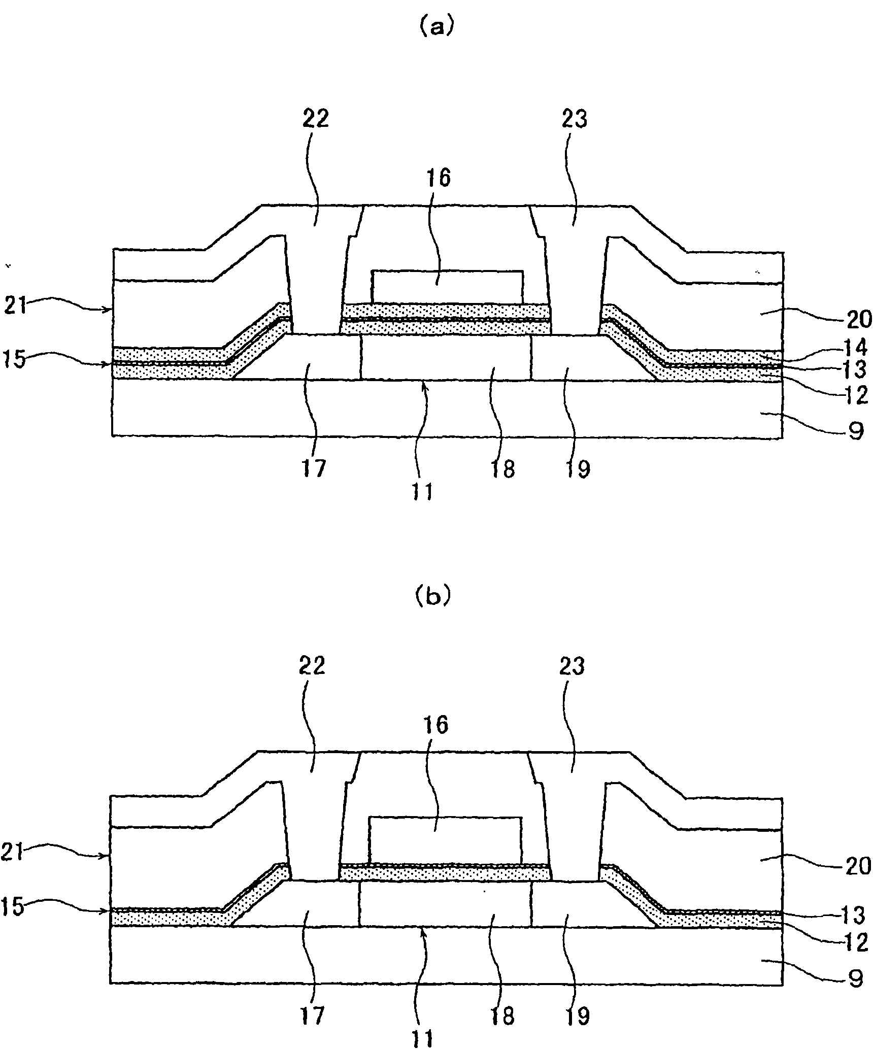
[0052] Hereinafter, the present invention will be described based on the illustrated embodiments.
[0053] figure 1 It is a schematic cross-sectional view showing a low-temperature polysilicon TFT (hereinafter referred to as a polysilicon TFT) as a thin film transistor formed by the manufacturing method of the present invention, wherein (a) indicates that the gate insulating layer is a first silicon oxide film, a silicon nitride film and a three-layer laminated structure of a second silicon oxide film; (b) shows a two-layer laminated structure of a first silicon oxide film and a silicon nitride film.
[0054] refer to figure 1 (a), the thin film transistor of the present embodiment includes an active layer 11 including a source region 17, a drain region 19, and a channel region 18 on a substrate 9, and a gate electrode layer 16, and the active layer 11 and the gate electrode layer 16 The gate insulating layer 15 formed between them; the gate insulating layer 15 includes a ...
PUM
 Abstract
Description
Claims
Application Information