Multi-layer flexible printed circuit board and method of manufacturing the same

A flexible printing and manufacturing method technology, which is applied in multilayer circuit manufacturing, printed circuit components, semiconductor/solid-state device manufacturing, etc. Flatness, cheap and stable manufacturing, effect of reducing vias

Inactive Publication Date: 2009-10-28
NIPPON MEKTRON LTD
View PDF1 Cites 10 Cited by
  • Summary
  • Abstract
  • Description
  • Claims
  • Application Information

AI Technical Summary

Problems solved by technology

[0025] Therefore, there is a problem that it is difficult to ensure the reliability of the interlayer connection of the laminated layer, or the size of the substrate during curing is relatively large due to the thick laminated adhesive material, and it is difficult to manufacture even an 8-layer structure. Multilayer flexible printed circuit board with high density CSP

Method used


Image

  • Multi-layer flexible printed circuit board and method of manufacturing the same
  • Multi-layer flexible printed circuit board and method of manufacturing the same
  • Multi-layer flexible printed circuit board and method of manufacturing the same

Examples


Embodiment 1

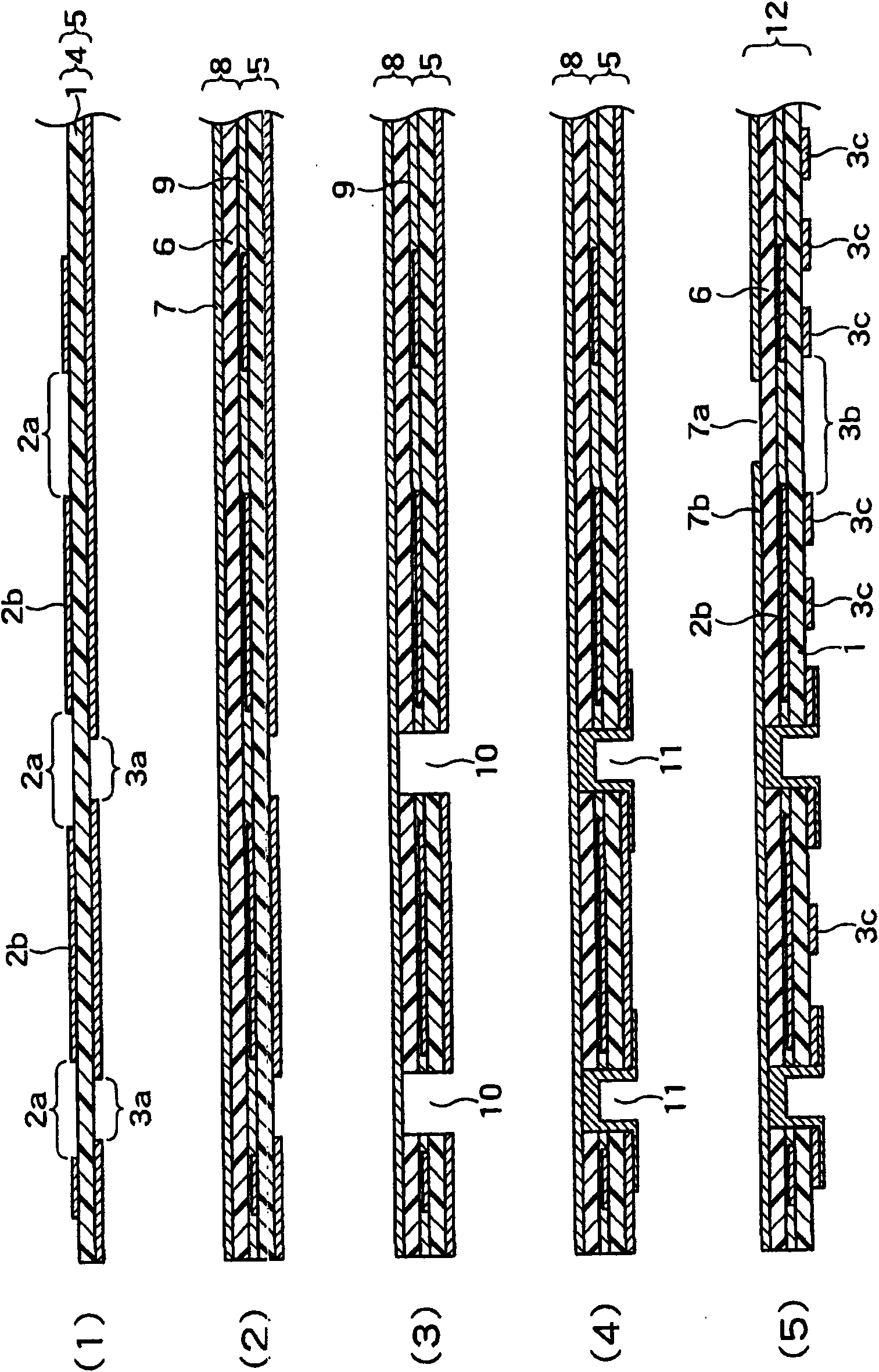
[0109] Figure 1A ~ Figure 1D It is a process drawing which shows the manufacturing method of this invention. A method of manufacturing a multilayer flexible printed wiring board having an 8-layer structure having a cable portion will be described with reference to this process diagram.

[0110] First, if Figure 1A As shown in (1), in the double-sided copper-clad laminate 4, a conformal mask 2a and a circuit pattern 2b are formed at the time of laser processing of the copper foil 2 on the inner layer side. As the double-sided copper-clad laminate 4, for example, a flexible insulating base material 1 (here, polyimide with a thickness of 12.5 μm) having copper foils 2 and 3 with a thickness of 12 μm on both sides of polyimide or the like is used. .

[0111] The conformal mask 2a and the circuit pattern 2b are formed by etching the copper foil 2 by metal surface photofabrication. Moreover, the conformal mask 3a at the time of laser processing is formed on the copper foil 3 u...

Embodiment 2

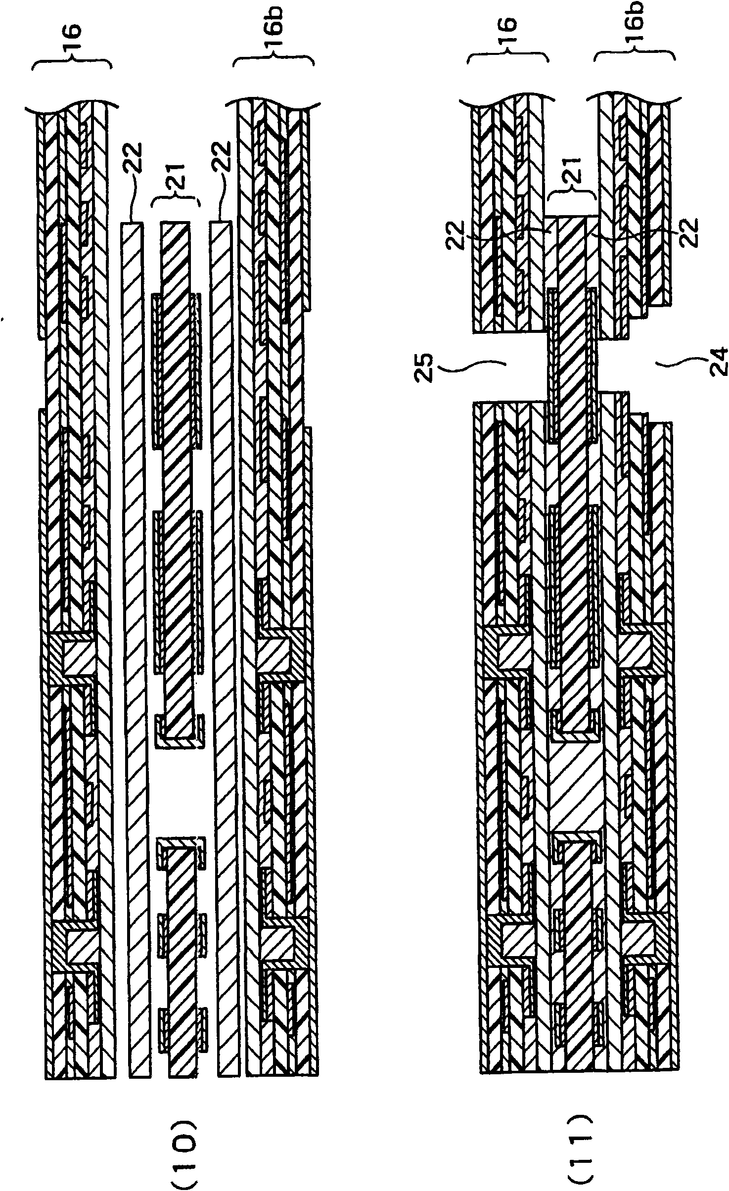
[0143] image 3 It is a sectional view showing the structure of the second embodiment of the present invention. as it should image 3 As shown, by changing the position where part of the build-up layer 16b was removed when producing the build-up layer 16b, the cable part of the outer layer can be formed on the circuit 35 of the second conductive layer in a single layer. Thus, an 8-layer flexible printed wiring board 37 having single-layer cables on the outer layer is obtained.

[0144] By employing such a cable structure, it can be suitably applied to a site requiring flexibility, such as a hinge portion of a mobile phone. Additionally, by image 3 Combining the through vias 38 in that way also enables direct connection of all layers.

Embodiment 3

[0146] Figure 4 It is a sectional view showing the structure of the third embodiment of the present invention. as it should Figure 4 As shown, a part of the build-up layer remains and is stacked in a bent state, whereby the circuit 39 of the third conductive layer 3 can also be directly connected to the third conductive layer 3' on the opposite surface, and it can be effectively mounted. The signal of the third conductive layer 3 of the signal layer of the component on the first conductive layer 7 is connected to the third conductive layer 3 ′ (opposite signal layer) on the opposite side.

[0147] In addition, as an interlayer connection connecting four layers, a via hole 40 (connecting the first conductive layer 7 and the core substrate 21), a stepped via hole 41 (connecting the first conductive layer 7', the third conductive layer 3 'and the core substrate 21), stepped vias 27 (connecting the first conductive layer 7', the second conductive layer 2', the third conductive...


PUM


Abstract

The present invention provides a multi-layer flexible printed circuit board which is capable of carrying narrow space length high-density CSP and a method for manufacturing the same. The multi-layer flexible printed circuit board comprises a three-layered structure lamination layer on at least one single surface of a core substrate of which two surfaces are provided with wiring pattern, and is characterized in that the a first conductive layer (7) of the first layer from the outer side of the lamination layer is provided with an installation solder pad (34) for installing a chip level packaging, a second conductive layer (2) of the second layer from the outer side of the lamination layer is provided with a grounding layer which at least is below the zone carrying the chip level packaging, a third conductive layer of the third layer from the outer side of the lamination layer is provided with wiring pattern for leading and winding a signal circuit, the wiring pattern is conducted by jumping a jumping conducting hole (28) of the grounding layer of the second conductive layer from the installation solder pad, the jumping conducting hole is a blind hole with a bottom and the bottom is connected with the back surface of the installation solder pad of the first conductive layer, and the multi-layer flexible printed circuit board is also provided with a conducting holes (40) of the conducting lamination layer and the core substrate (21) besides the jumping conducting hole, and a flexible cable part which is integrated with the lamination layer.

Description

technical field [0001] The present invention relates to a multilayer flexible printed wiring board and a manufacturing method thereof, and more particularly to a build-up type multilayer flexible printed wiring board having a flexible cable portion and a manufacturing method thereof. Background technique [0002] In recent years, electronic devices, especially mobile phones, have rapidly advanced in functionality. Along with this, there has been a trend that components mounted on multilayer flexible printed wiring boards are also replaced with chip-scale packages (Chip-Size Package, also It is called Chip-Scale Package (hereinafter referred to as CSP), and it is packaged with high functionality and high density, and high functionality can be added without greatly increasing the size of the substrate. [0003] The pad pitch of this CSP was initially 0.8 mm, but in recent years there has been a demand for a narrower pitch of 0.4 mm or less. In particular, it is very difficult...

Claims


Application Information

Patent Timeline
Patent Type & Authority Applications(China)
IPC IPC(8): H05K1/02H05K3/46H01L23/498H01L21/48
CPCH01L2924/0002
Inventor 松田文彦
Owner NIPPON MEKTRON LTD
Why Eureka
Try Eureka