

Chemical mechanical planarization composition, system, and method of use
A compound, planarization technology, applied in chemical instruments and methods, other chemical processes, machine tools suitable for grinding workpiece planes, etc., can solve the problems of scratching the surface of the wafer, dishing the wafer surface, and messy slurry. Achieve the effect of reducing dishing, increasing selectivity ratio, and high removal rate
Inactive Publication Date: 2009-10-28
3M INNOVATIVE PROPERTIES CO
View PDF4 Cites 5 Cited by
- Summary
- Abstract
- Description
- Claims
- Application Information
AI Technical Summary
Problems solved by technology
[0004] However, one drawback of slurry-based CMP processing is that the slurry grinding process must be carefully monitored to achieve the desired topography of the wafer surface and avoid dishing on the wafer surface
The second drawback is that slurries using loose abrasives have the potential to scratch the wafer surface
Another drawback is the mess caused by the slurry and the large amount of abrasive particles on the wafer surface that must be removed and disposed of during subsequent wafer processing
Handling and disposing of these slurries creates additional processing costs for semiconductor wafer manufacturers
Method used
View moreImage
Smart ImageViewing Examples

Examples
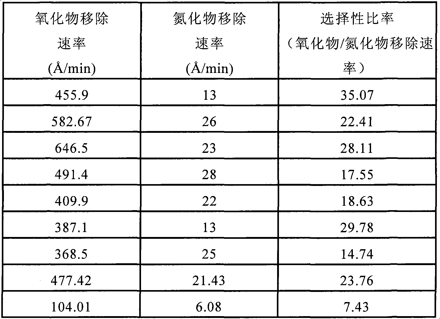
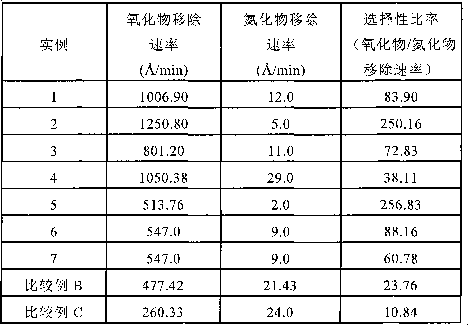
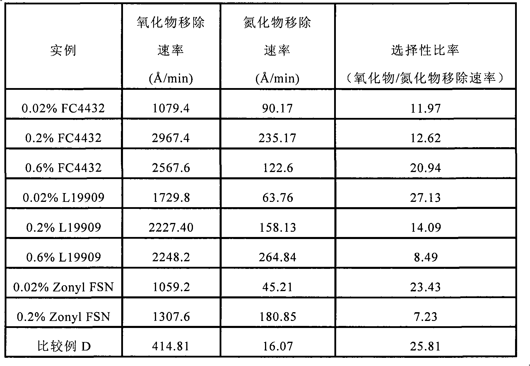
example
[0047] The material designations shown in Table 1 were used for all examples. All compositional percentages in the following examples are expressed in weight percentages of the working fluid.
[0048] Table 1: Fluorochemical Surfactants Used in the Examples
[0049] name
example 1
[0056] A working solution containing 0.02% Zonyl FSN and 2.5% L-proline at a pH of 10.5 yielded 1006.90 / min average oxide removal rate, 12.0 / min nitride removal rate and selectivity ratio of 83.9.
example 2
[0058] A working solution containing 0.2% Zonyl FSN and 2.5% L-proline at a pH of 10.5 yielded 1250.80 / min average oxide removal rate, 5.0 / min nitride removal rate and selectivity ratio of 250.16.
Login to View More PUM
| Property | Measurement | Unit |
|---|---|---|
| diameter | aaaaa | aaaaa |
Abstract
The disclosure relates to chemical mechanical planarization (CMP) polishing compositions including proline and a fluorochemical surfactant. The wafer polishing composition may be used as a solution substantially free of abrasive particles, the composition of which can be adjusted to control Oxide Removal Rate and oxide over nitride Selectivity Ratio in Shallow Trench Isolation (STI) processing ofsemiconductor wafers using a fixed abrasive CMP process. In certain embodiments, the disclosure provides a working liquid for fixed abrasive CMP including proline and a fluorochemical surfactant at apH from 9 to 11. When used in a fixed abrasive CMP system and method for STI, exemplary working liquids may yield an Oxide Removal Rate of at least 500 angstroms per minute, and an oxide over nitrideSelectivity Ratio of at least 5.
Description
technical field [0001] The present invention generally relates to compositions for chemical-mechanical planarization (CMP). More particularly, the present invention relates to compositions useful with fixed abrasive articles in CMP systems and methods. Background technique [0002] During the fabrication of integrated circuits, semiconductor wafers used for semiconductor fabrication typically go through multiple steps including deposition, patterning and etching steps. Details of these manufacturing steps for semiconductor wafers are published by Tonshoff et al. in Annals of the International Institution for Production Engineering Research (Annual Report of the International Production Engineering Research Society), (Vol. Machining ofSilicon" (grinding of silicon) has been reported. During each fabrication step, it is often necessary or desirable to alter or refine the exposed surface of the wafer in order to prepare the wafer for subsequent fabrication or preparation step...
Claims
Login to View More Application Information
Patent Timeline
 Patent Type & AuthorityApplications(China)
IPC IPC(8): C09K3/14
CPCC09G1/04B24B7/228H01L21/31053C09K3/14
Inventor约翰·J·加格里亚蒂帕特里西亚·M·萨武
Owner3M INNOVATIVE PROPERTIES CO