Location test system for defects of integrated circuit and implementation method thereof

A technology of integrated circuits and testing systems, applied in the field of positioning and testing of integrated circuit defects, can solve problems such as inability to achieve positioning, and achieve the effects of speeding up research and development, accurately discovering, and improving product quality

Inactive Publication Date: 2009-11-11
SHANGHAI FALAB TEST
View PDF0 Cites 20 Cited by
  • Summary
  • Abstract
  • Description
  • Claims
  • Application Information

AI Technical Summary

Problems solved by technology

[0002] For the defect location of integrated circuits, low-light radiation location technology is generally used at present. This technology uses the electron-hole pair coupling at the defect site to release photons to detect the failure point. This technology has obvious limitations. , short circuit, and defect points below the aluminum wire covering parts cannot be located

Method used


Image

  • Location test system for defects of integrated circuit and implementation method thereof
  • Location test system for defects of integrated circuit and implementation method thereof
  • Location test system for defects of integrated circuit and implementation method thereof

Examples


Embodiment Construction

[0032] The present invention will be further described below with reference to the accompanying drawings.

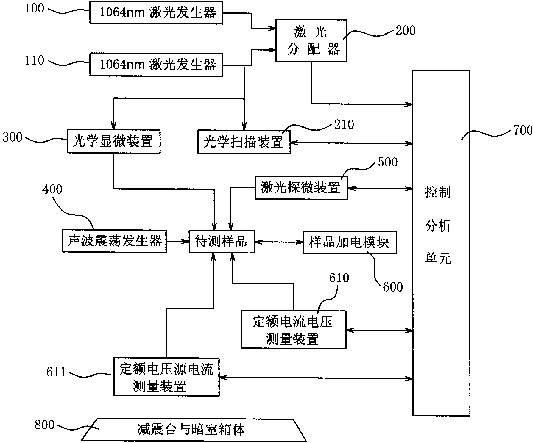
[0033] Explanation of the number labels in the figure:

[0034] 100-1064 nanometer laser generator, 110-1340 nanometer laser generator, 200-laser distributor, 210-laser scanning device; 300-optical microscope device, 400-ultrasonic vibration generator, 500-low-light detection device; 600 - sample power supply module, 610 - rated current and voltage measuring device; 611 - rated voltage source current measuring device, 700 - control analysis unit, 800 - shock absorption table and darkroom box, 900 - sample to be tested.

[0035] figure 1 instruction of:

[0036] As shown in the figure, the structure of the integrated circuit defect location testing system is as follows: the control analysis unit 700 is the main user-oriented operation interface in the system, which plays an image analysis and overall control role in the entire testing process; The laser distributor 200...


PUM


Abstract

The invention provides a location test system for defects of an integrated circuit and an implementation method thereof, belonging to the field of electronic test equipment, and relating to a system for locating and testing the defects of the integrated circuit and an implementation method thereof. The system mainly comprises a control analysis unit, a laser generator, a laser distribution device,a laser scanning device, an acoustic oscillation generator, an optical microscope device, a sample electrification module, a weak light detection device, a rated current voltage measurement device, arated voltage current measurement device, a damping platform, a darkroom case, and the like. Due to the adoption of the invention, the physical position of various defects of the integrated circuit can be located intuitively, and the defects of the integrated circuit can be found in time and accurately so as to improve the product quality, accelerate the speed of research and development and improve the production technique level.

Description

technical field [0001] The invention belongs to the field of electronic testing equipment, and relates to a system for positioning and testing integrated circuit defects and a method for realizing the system. Background technique [0002] For the defect location of integrated circuits, low-light radiation location technology is generally used at present. This technology uses the electron-hole pair coupling at the defect site to release photons to detect the failure point. This technology has obvious limitations. , short circuit, and defect points under the aluminum wire covering parts cannot be located. [0003] The present invention innovates defect location technology by combining ultrasonic and laser beams (for example: wavelength: 1.3um, energy: 100mW, focus point: 0.65um) to scan silicon crystals, resulting in local heating, and using ultrasonic waves to strengthen heat accumulation Effect, and observe its current change to locate the defect points that may have proble...

Claims


Application Information

Patent Timeline
Patent Type & Authority Applications(China)
IPC IPC(8): G01N35/00G01N21/956G01N29/02G01R31/02G01R31/28
Inventor 刘学森
Owner SHANGHAI FALAB TEST
Why Eureka
Try Eureka