Manufacturing method of a piezoelectric micro-cantilever beam probe

A technology of a micro-cantilever beam and a manufacturing method, which is applied to piezoelectric devices/electrostrictive devices and other directions, can solve the problems of influence, small probe sharpness, and poor needle tip quality, and achieves cost reduction, low process equipment requirements, and maintenance sharpness effect

Inactive Publication Date: 2011-04-27
DALIAN UNIV OF TECH
View PDF0 Cites 0 Cited by
  • Summary
  • Abstract
  • Description
  • Claims
  • Application Information

AI Technical Summary

Problems solved by technology

However, the sharpness of the probe produced by this method is small, and the shape of the tip is affected by the shape of the mold, and the quality of the tip is poor

Method used


Image

  • Manufacturing method of a piezoelectric micro-cantilever beam probe
  • Manufacturing method of a piezoelectric micro-cantilever beam probe
  • Manufacturing method of a piezoelectric micro-cantilever beam probe

Examples


Embodiment 1

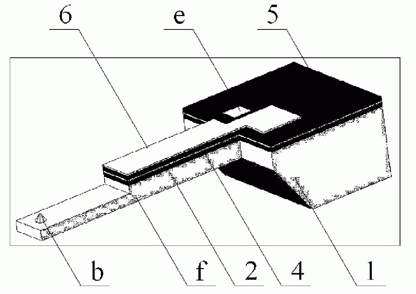
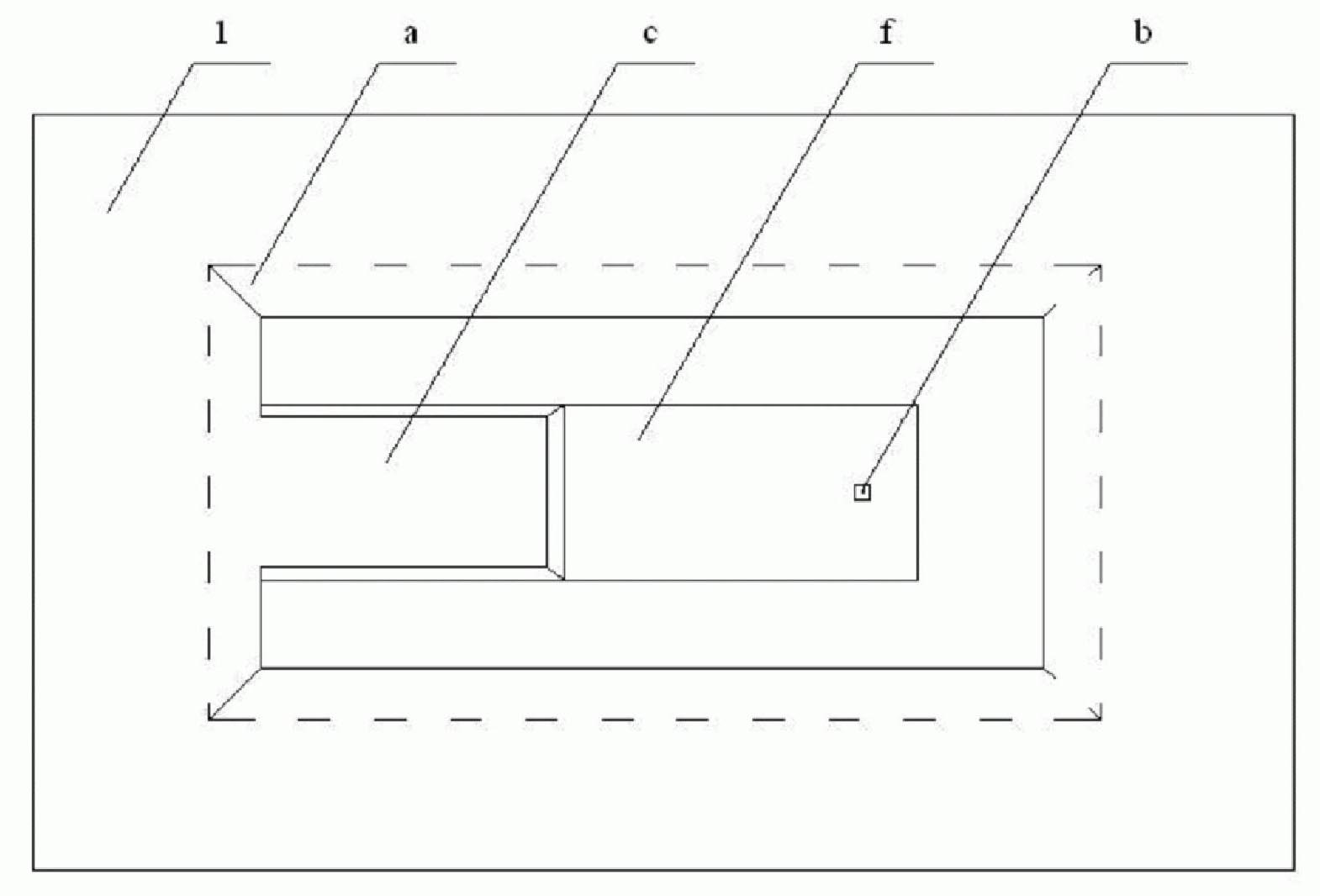
[0043] For the piezoelectric micro-cantilever probe in this embodiment, the length and width of the micro-cantilever are 450 microns and 70 microns, and the tip height is 5 microns. A micro-cantilever beam probe was fabricated using n-type (100) double-sided polished single-crystal silicon wafers with a thickness of 220 microns. Its specific production process is as follows:

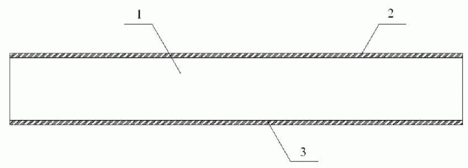
[0044] Conventional thermal oxidation monocrystalline silicon wafer 1 forms upper surface silicon dioxide layer 2 and lower surface silicon dioxide layer 3 on single crystal silicon wafer, and the thickness of oxide layer is about 1.3 microns (attached Figure 3.1 ).

[0045] Silicon wafer back treatment process: Rectangular windows are photolithographically etched on the back, and silicon dioxide is etched with hydrofluoric acid buffer solution (BHF), and a rectangular window pattern 3' with silicon dioxide removed is produced (attached Figure 3.2 );

[0046] Use potassium hydroxide (KOH) anisotropic ...


PUM

PropertyMeasurementUnit
thicknessaaaaaaaaaa

Abstract

The invention discloses a manufacturing method of a piezoelectric micro-cantilever beam probe, belonging to the technical field of micro-mechanical sensors and actuators. The invention is characterized in that a partial piezoelectric layer is adopted to realize integration of the manufacturing technique of a nano silicon needle point and the manufacturing technique of a piezoelectric film. In themanufacturing process, the nano silicon needle point adopts anisotropic wet corrosion method with a mask; the piezoelectric film is manufactured by adopting a sol-gel method. The invention has the beneficial effects of having both functions of sensing and executing by adopting the piezoelectric film as a sensitive part, being capable of finishing the whole technological process by adopting a dry etching and wet etching technique, having lower requirements on the technological equipment, being capable of being produced in batches and reducing the cost of products. The piezoelectric micro-cantilever beam probe manufactured by the method can be used for atomic force microscopes, nano-imprint storage devices and field emission devices.

Description

technical field [0001] The invention belongs to the field of micromechanical sensors and actuators, and relates to a manufacturing method of a piezoelectric micro-cantilever beam probe, which is suitable for atomic force microscope (AFM) probes, high-density storage device probes and micro-nano processing devices. Background technique [0002] The atomic force microscope is a high-definition surface analyzer newly developed in recent years. This surface analysis instrument observes the surface structure of the sample by detecting the change of the weak interatomic force between the needle tip and the sample surface. AFM can not only observe the surface morphology of conductive materials, but also observe the surface morphology of non-conductive materials. Therefore, it has become a powerful tool for humans to observe and study the microscopic world. [0003] The traditional AFM is mainly a laser detection-like atomic force microscope. The key part is a force sensor compose...

Claims


Application Information

Patent Timeline
Patent Type & Authority Patents(China)
IPC IPC(8): H01L41/08
Inventor 崔岩夏劲松赵佳欣张吕权王立鼎
Owner DALIAN UNIV OF TECH
Why Eureka
Try Eureka