Compound encapsulation structure and method of organic electroluminescence device

A technology of electroluminescent devices and packaging structures, applied in the direction of electric solid devices, electrical components, semiconductor devices, etc., can solve the problems that restrict the practical application of thin film packaging, damage to light-emitting devices, etc., achieve high resistivity, reduce damage, and simple operation Effect

Inactive Publication Date: 2009-11-18
SHANGHAI UNIV
View PDF0 Cites 17 Cited by
  • Summary
  • Abstract
  • Description
  • Claims
  • Application Information

AI Technical Summary

Problems solved by technology

The deposition process of the above-mentioned inorganic materials will cause different degrees of damage to the organic electroluminescent device, which restricts the practical application of thin film encapsulation

Method used


Image

  • Compound encapsulation structure and method of organic electroluminescence device
  • Compound encapsulation structure and method of organic electroluminescence device

Examples


Embodiment 1

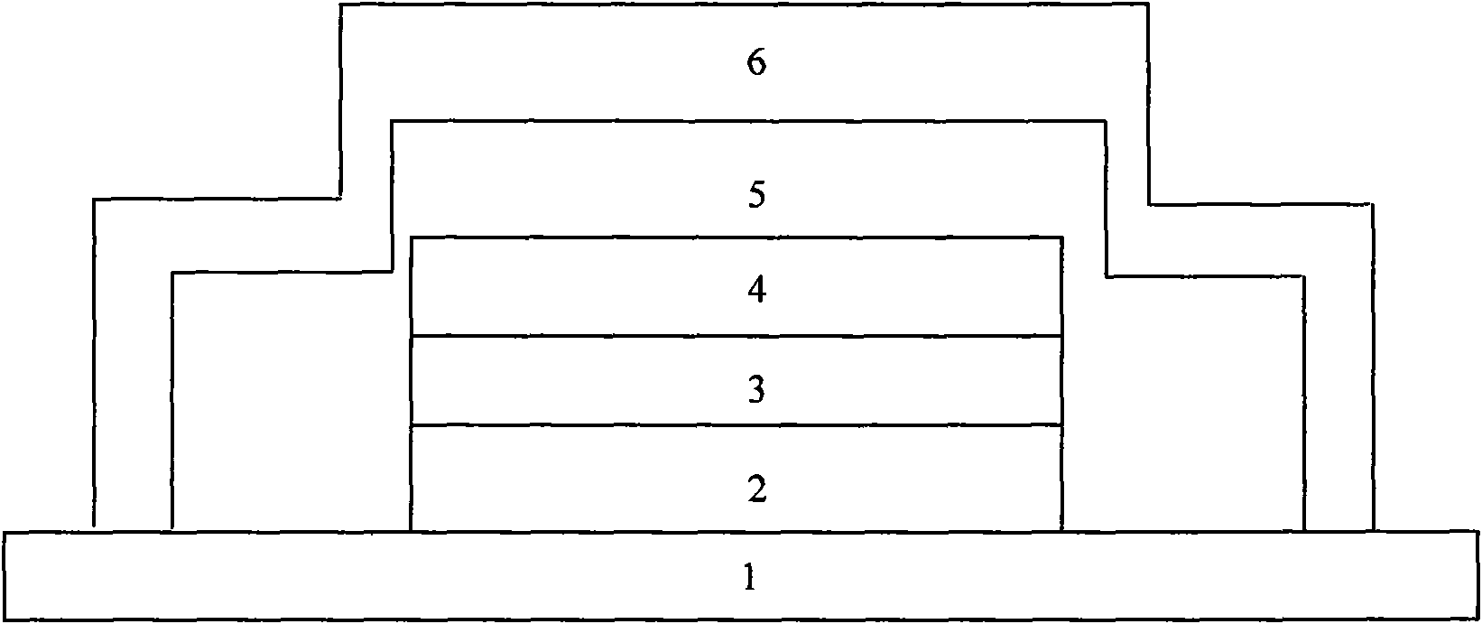
[0023] Such as figure 1 As shown, the composite packaging structure of the glass organic electroluminescent display device includes a substrate 1, an ITO film 2, an organic electroluminescent material layer 3, a metal layer 4, a packaging buffer layer 5, and a packaging layer 6. The ITO thin film 2 is fabricated on the substrate 1, the organic electroluminescent material layer 3 is fabricated on the ITO thin film 2, the metal layer 4 is deposited on the organic layer 3 by thermal evaporation, and the packaging buffer layer 5 is fabricated on the metal layer 4. On, finally make encapsulation layer 6. By connecting the positive electrode ITO film and the negative electrode metal electrode layer, the organic material layer is passed a direct current to drive light emission.

[0024] The preparation method of this composite encapsulation layer is as follows: adopt LiF material as encapsulation buffer layer 5, use and prepare the same evaporation equipment of OLED device, the evap...

Embodiment 2

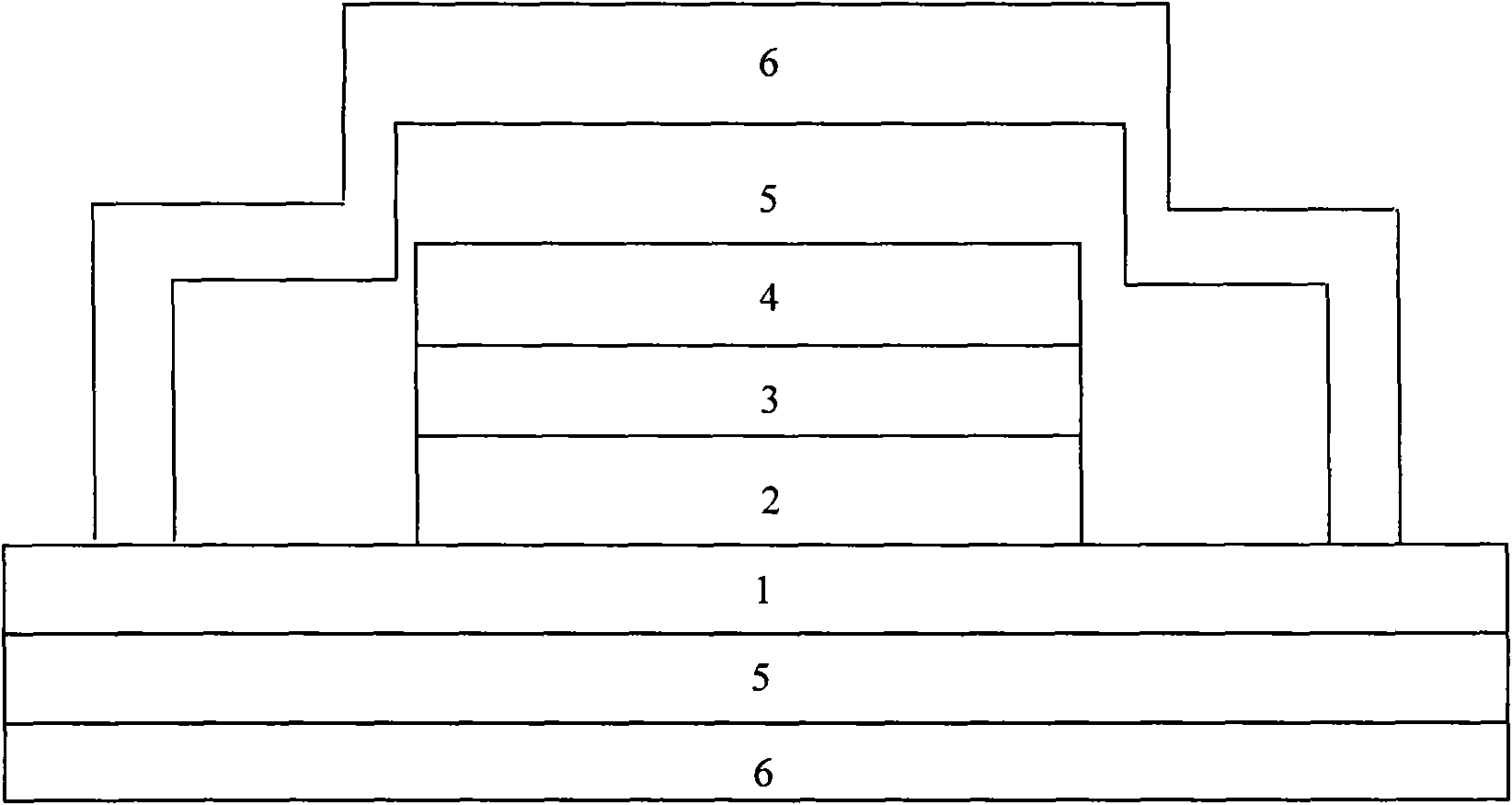
[0030] Embodiment two: if figure 2 As shown, the present embodiment is basically the same as the first embodiment, except that the buffer layer 5 and the encapsulation layer 6 are also prepared on the back surface of the substrate 1 (the surface without ITO).


PUM


Abstract

The invention relates to a new compound encapsulation structure and a method of an organic electroluminescence device. The compound encapsulation structure comprises a substrate and an ITO membrane, an electroluminescence material layer and an encapsulation layer which are overlaid on the substrate in sequence, wherein, the encapsulation layer is arranged on a metal layer and is used for retaining water vapor and oxygen. The inner side of the encapsulation layer is provided with a buffer layer which is used for assistant encapsulation and further retaining the water vapor and oxygen with the encapsulation layer together, thus forming the compound encapsulation structure. The preparation steps of the method include: (1) adopting vacuum evaporated LiF layer to prepare the buffer layer; and (2) preparing the encapsulation layer on the LiF layer. The compound encapsulation structure can improve the action of retaining the water vapor and oxygen, and the method is easy to operate with low cost.

Description

technical field [0001] The invention relates to a thin film packaging structure and method of an organic electroluminescent device, which can be used as an auxiliary packaging means for the organic electroluminescent device, in particular to a film composite packaging structure and method of the organic electroluminescent device. Background technique [0002] Organic Light Emitting Device (OLED) is widely used in flat panel displays, backlight modules and lighting due to its characteristics of ultra-thin, high brightness, fast response, low power consumption, high efficiency and simple production. The principle of luminescence is to deposit a very thin organic material between two electrodes, and apply direct current to the organic luminescent material to make it luminous. [0003] Using a substrate with high light transmission and strong flexibility as the anode substrate to prepare flexible OLED (FOLED) has the advantages of more impact resistance, light weight and thinner...

Claims


Application Information

Patent Timeline
Patent Type & Authority Applications(China)
IPC IPC(8): H01L51/52H01L51/56H01L23/31H01L23/29H01L21/56
Inventor 魏斌路林李博张浩张建华汪敏
Owner SHANGHAI UNIV
Why Eureka
Try Eureka