Packaging method used for high-power integrated circuit

An integrated circuit and packaging method technology, applied in the field of semiconductor packaging manufacturing, can solve the problems of poor heat dissipation, affecting heat dissipation, and large thermal resistance.

Active Publication Date: 2009-12-02
WUXI YOUDA ELECTRONICS
View PDF0 Cites 15 Cited by
  • Summary
  • Abstract
  • Description
  • Claims
  • Application Information

AI Technical Summary

Problems solved by technology

This type of package has a lower cost due to the smaller copper base, but the heat dissipation effect is poor, because the copper base is not in direct contact with the heat sink, but is in contact with the heat sink through the metal substrate, so the thermal resistance is large, which affects heat dissipation

Method used


Image

  • Packaging method used for high-power integrated circuit
  • Packaging method used for high-power integrated circuit
  • Packaging method used for high-power integrated circuit

Examples


Embodiment Construction

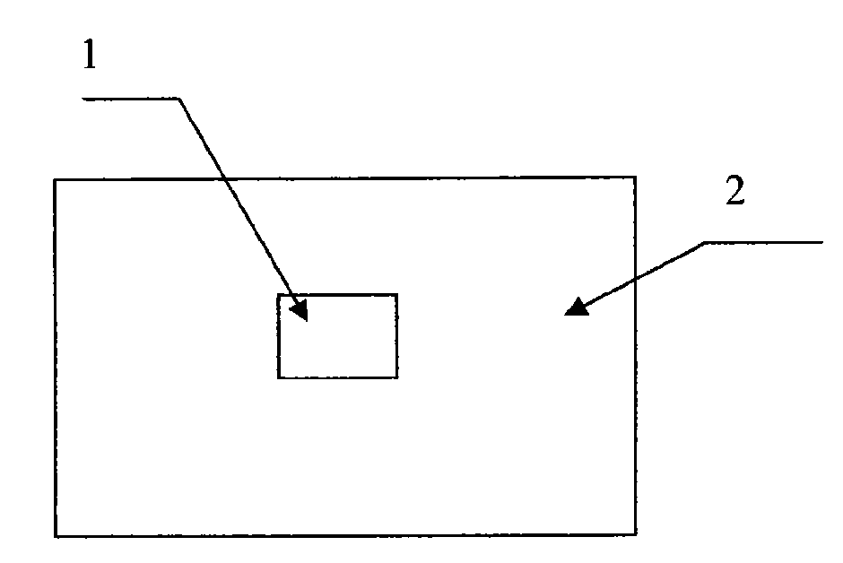
[0029] The packaging process for high-power integrated circuits adopts metal base embedded metal substrate packaging, and the specific implementation methods are as follows:

[0030] 1. Drill a hole on the metal substrate with a size slightly smaller than the metal base,

[0031] 2. Embed the metal base into the metal substrate,

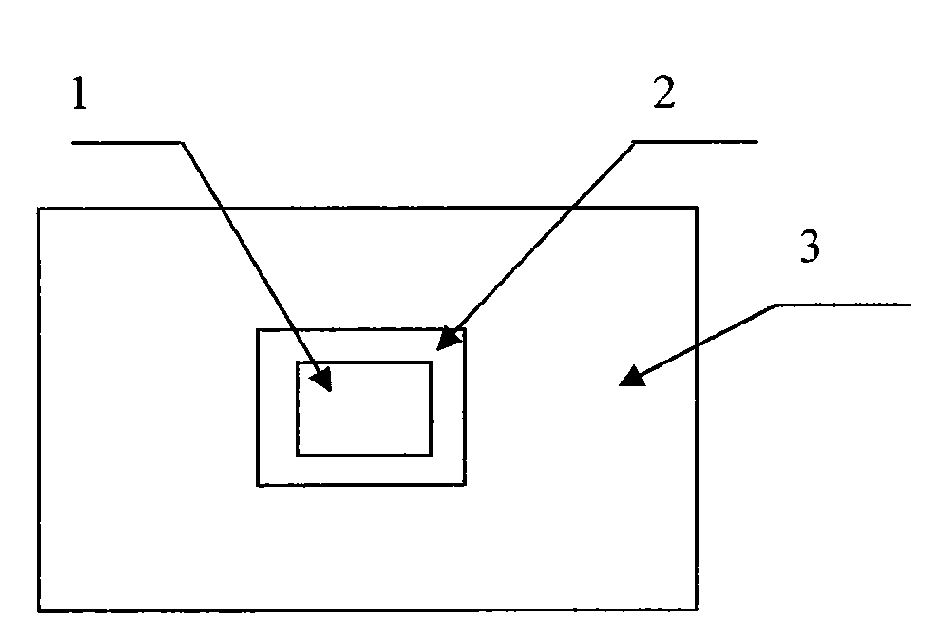
[0032] 3. Print solder paste on metal base and metal substrate,

[0033] 4. Install the chip and lead pins on the metal base and metal substrate respectively,

[0034] 5. Put the chip, lead pins, metal base and metal substrate together in a sintering furnace for sintering at a temperature of 210°C~230°C.

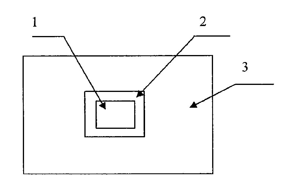
[0035] 6. The chip and the lead pin are bonded by wire,

[0036] 7. Check under the microscope whether there is detachment or missing bonding,

[0037] 8. Coat the surface of the chip with glue,

[0038] 9. Seal the case, cover the metal substrate with a case,

[0039] 10. Cut the ribs and bend the leads,

[0040] 11. Test open and short cir...


PUM


Abstract

The invention discloses a packaging method for a high-power integrated circuit, which adopts a packaging manufacturing process for inserting a metal base into a metal substrate. During the package, the method comprises the following steps: firstly, punching a hole of which size is slightly smaller than the size of the metal base on the metal substrate, and inserting the base into the hole of the substrate; secondly, sintering a chip and the base by soldering paste, and sintering a terminal pin and the substrate by the soldering paste; and bonding the chip and the terminal pin, and finally carrying out pouring molding and packing. In the conventional package process, because the metal base is contacted with an outer radiating fin through the metal substrate, the thermal resistance is large, and the heat dissipation is slow; and by adopting the package process for inserting the metal base into the metal substrate, the metal base is directly contacted with the radiating fin, so the thermal resistance is small, and the heat dissipation is quick.

Description

technical field [0001] The invention relates to an advanced packaging technology used in an integrated circuit with relatively large output power, and belongs to the technical field of semiconductor packaging production. Background technique [0002] As we all know, the current international semiconductor integrated circuits are developing in two directions: one is low-voltage and low-power integrated circuits represented by CMOS and BiCMOS; the other is high-voltage and high-power integrated circuits represented by DMOS and Bipolar. For the first type of circuit, because of its small output power, there is almost no requirement for the heat dissipation of the package; for the latter circuit, because of its large output power, it will inevitably generate more heat, so there is no requirement for the heat dissipation of the package. higher requirements. If the heat dissipation of the package is poor, the temperature of the chip will rise rapidly, and the circuit will enter t...

Claims


Application Information

Patent Timeline
Patent Type & Authority Applications(China)
IPC IPC(8): H01L21/50H01L21/60H01L21/48
Inventor 朱伟民邓晓军聂卫东卜惠琴
Owner WUXI YOUDA ELECTRONICS
Why Eureka
Try Eureka