
A universal method for selective area growth of organic molecules by vapor deposition

An organic molecule, vapor phase deposition technology, applied in the direction of crystal growth, single crystal growth, single crystal growth, etc., can solve the problems of patterning and processing of organic semiconductor devices that have not been used before, and achieve effective raw material utilization rate, high resolution, low cost effect

Inactive Publication Date: 2009-12-30
WESTFALISCHE WILHELMS UNIV MUNSTER
View PDF1 Cites 19 Cited by
  • Summary
  • Abstract
  • Description
  • Claims
  • Application Information

AI Technical Summary

Problems solved by technology

However, selective growth techniques have not been used for patterning and processing of organic semiconductor devices

Method used


Image

  • A universal method for selective area growth of organic molecules by vapor deposition
  • A universal method for selective area growth of organic molecules by vapor deposition
  • A universal method for selective area growth of organic molecules by vapor deposition

Examples


Embodiment Construction

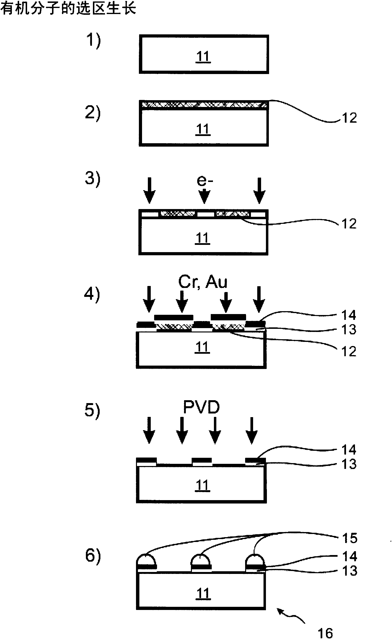
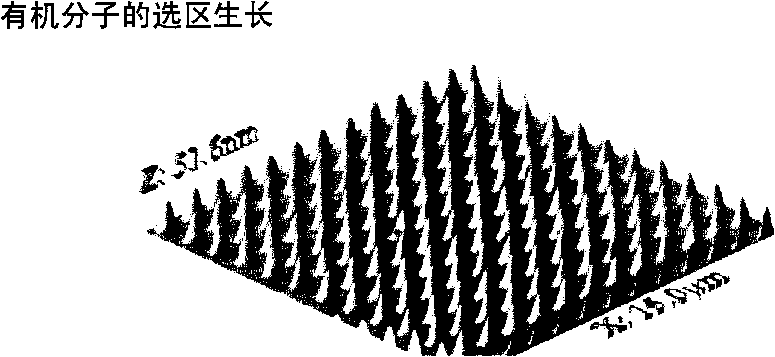
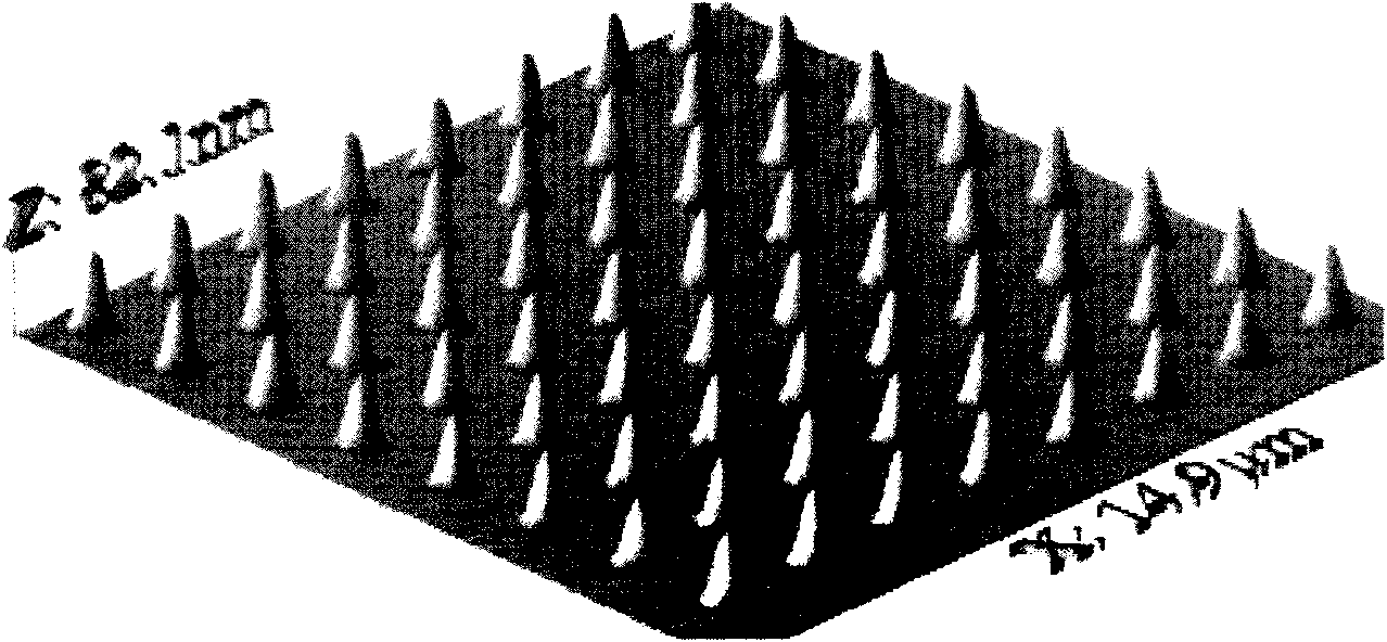
[0038] The present invention can be described by the theory of film growth kinetics. According to the interaction between molecules and solid substrates, there are three growth modes of molecules deposited on solid substrates: island growth, layer growth and layer plus island growth modes. Island-like growth patterns are observed when the interaction between the solid substrate and the molecules to be deposited is weak. Lamellar growth, on the other hand, occurs when the substrate and molecular interactions are comparable. The layer-plus-island growth mode is a combination of the above two modes, that is, the molecules grow in a layered mode in the first layer or layers, and then transform into an island-like growth mode, which corresponds to a stronger interaction between molecules and the solid substrate. effect. Layered growth modes can be achieved when the interaction between molecules and solid substrate is moderate. The growth mode and average diffusion length of mole...


PUM

PropertyMeasurementUnit
diameteraaaaaaaaaa

Abstract

A method for selective growth of organic molecules on a substrate is proposed. The method comprises: creating a pattern of nucleation sites for the organic molecules on the substrate; depositing of organic molecules at the nucleation sites by vapor deposition. An organic material based device obtained by performing the method is also proposed. The method offers an alternative to methods that are known the fields of coating technology or semiconductor fabrication.

Description

technical field [0001] The invention relates to a method for selective growth of organic molecules on a substrate. [0002] The invention further relates to devices based on organic materials fabricated by this method. Background technique [0003] Group IV and III-V inorganic semiconductors have played a mainstay role in the semiconductor industry for nearly five decades. However, organic semiconductors have received considerable attention in recent years due to their ease of processing and potential low cost compared to the same inorganic semiconductors. Organic semiconductors are used in organic light emitting diodes (OLEDs), organic field effect transistors (OFETs), optoelectronic devices, and organic semiconductor lasers. Some products based on organic semiconducting materials have entered the market. However, its commercial prospects will largely depend on device fabrication and packaging, which determine product cost. [0004] In general, organic semiconductors ca...

Claims


Application Information

Patent Timeline
Patent Type & Authority Applications(China)
IPC IPC(8): C23C14/04C23C14/12C30B23/04C30B29/54
CPCC23C14/12H01L51/0011C30B29/54C23C14/042C30B23/04Y02E10/549H10K71/166C23C14/024C23C16/0272
Inventor 哈勒德·福克斯迟力峰王文冲钟定永
Owner WESTFALISCHE WILHELMS UNIV MUNSTER
Learn More