Film layer, manufacturing method thereof and photovoltaic device with film layer

A manufacturing method and film layer technology, applied in the field of solar cells, can solve the problems of increasing process difficulty and complexity, roughness, etc., to avoid sudden changes in the value of the light refraction index, reduce reflection and refraction loss, and have high controllability Effect

Active Publication Date: 2012-06-27
杨与胜 +1
View PDF0 Cites 0 Cited by
  • Summary
  • Abstract
  • Description
  • Claims
  • Application Information

AI Technical Summary

Problems solved by technology

In addition, in order to obtain a rough velvet surface (texture), it is necessary to use hydrochloric acid or hydrofluoric acid to treat the zinc oxide film after magnetron sputtering. These factors undoubtedly increase the difficulty and complexity of the process.

Method used


Image

  • Film layer, manufacturing method thereof and photovoltaic device with film layer
  • Film layer, manufacturing method thereof and photovoltaic device with film layer
  • Film layer, manufacturing method thereof and photovoltaic device with film layer

Examples


Embodiment Construction

[0037] In order to make the above objects, features and advantages of the present invention more comprehensible, specific implementations of the present invention will be described in detail below in conjunction with the accompanying drawings. In the following description, numerous specific details are set forth in order to provide a thorough understanding of the present invention. However, the present invention can be implemented in many ways other than those described here, and those skilled in the art can make similar extensions without departing from the connotation of the present invention. Accordingly, the invention is not limited to the specific implementations disclosed below.

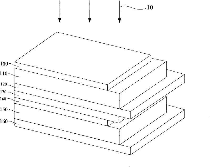
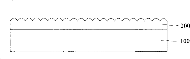
[0038] The transparent conductive front electrode of the thin film photovoltaic device not only requires a light transparency higher than 80% and a higher electrical conductivity, but also has a higher surface roughness (texture, also known as velvet), so that it has a nearly 10 % or higher, the...


PUM

PropertyMeasurementUnit
thicknessaaaaaaaaaa
thicknessaaaaaaaaaa
refractive indexaaaaaaaaaa

Abstract

The invention discloses a film layer, a manufacturing method thereof and a photovoltaic device with the film layer, which belong to the technical field of solar cells. By using magnetron sputtering technology, a laminated structure of a titanium oxide film, a silicon oxide film and a tin oxide film which are orderly deposited on the surface of a substrate is used as a front electrode of a transparent conductive oxide, so that the front electrode of the laminated transparent conductive oxide can be manufactured in multi-chamber sputtering equipment on line to improve the production efficiency and reduce the manufacturing cost.

Description

technical field [0001] The invention relates to the technical field of solar cells, in particular to a film layer, a manufacturing method thereof and a photovoltaic device with the film layer. Background technique [0002] Along with the day by day shortage of energy, the utilization of solar energy is subjected to people's general attention day by day. Especially in recent years, the widespread application of thin-film photovoltaic devices based on hydrogenated amorphous silicon and nanocrystalline silicon in commercial and residential installations has shown great potential. For a schematic diagram of a typical thin-film photovoltaic device, see figure 1 , the thin film photovoltaic device sequentially includes a glass substrate 100, a transparent conductive oxide (TCO) front electrode 110 along the direction of the incident light 10, a hydrogenated silicon thin film p-i-n photoelectric unit, including a p layer 120, an intrinsic i layer 130 (light absorbing layer) and n...

Claims


Application Information

Patent Timeline
Patent Type & Authority Patents(China)
IPC IPC(8): H01L31/18H01L31/0224
CPCY02P70/50
Inventor 杨与胜
Owner 杨与胜
Why Eureka
Try Eureka