Photoelectronic device and manufacturing method thereof
A technology for optoelectronic devices and manufacturing methods, applied in circuits, electrical components, semiconductor devices, etc., can solve the problems of concentrated ohmic resistance injection current, poor heat dissipation of sapphire substrates, and inability to effectively improve the luminous efficiency of light-emitting diodes, so as to improve luminous efficiency. Effect
- Summary
- Abstract
- Description
- Claims
- Application Information
AI Technical Summary
Problems solved by technology
Method used
Image

Examples
no. 1 example
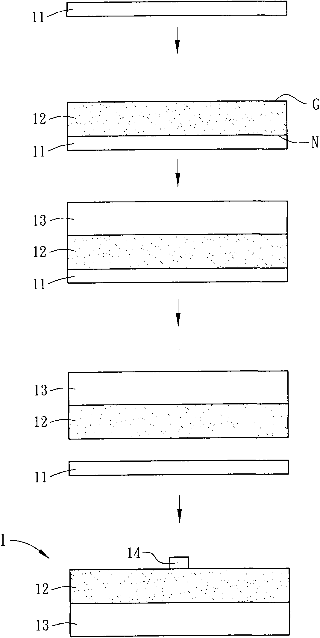
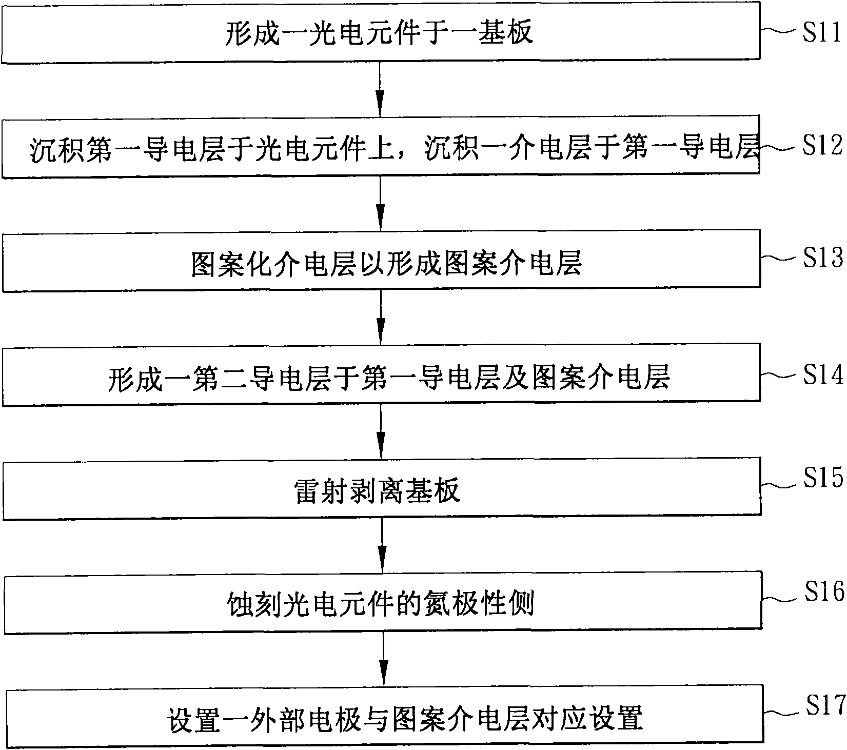
[0045] Please refer to figure 2 and image 3 As shown, a method for manufacturing an optoelectronic device according to the first embodiment of the present invention includes steps S11 to S17.
[0046] In step S11 , a photoelectric element 22 is formed on a substrate 21 . In this embodiment, taking the manufacture of blue light-emitting diodes as an example, the substrate 21 is a sapphire substrate, and the photoelectric element 22 is a group III or V compound semiconductor material. Generally speaking, the photoelectric element 22 can be made of a nitride series material such as a hexagonal gallium nitride (GaN) compound, and is formed on the substrate by a metalorganic chemical vapor deposition (MOCVD) or a molecular beam epitaxy (MBE) method. on the substrate 21. In addition, the photoelectric element 22 includes multiple semiconductor layers, and these semiconductor layers include an n-type semiconductor, a light-emitting layer and a p-type semiconductor layer. The ph...
no. 2 example
[0058] Please refer to Figure 4 and Figure 5 As shown, a method for manufacturing an optoelectronic device according to the second embodiment of the present invention includes steps S21 to S27.
[0059] In step S21 , a photoelectric element 32 is formed on a substrate 31 . Wherein, the materials and formation methods of the substrate 31 and the photoelectric element 32 are the same as the step S11 of the above-mentioned first embodiment, and will not be repeated here.
[0060] In step S22 and step S23 , a reflective ohmic contact film 33 is formed on the photoelectric element 32 . The reflective ohmic contact film 33 has a first conductive layer 331 and a patterned dielectric layer 332. In step S22, a dielectric layer (not shown) is deposited on the photoelectric element 32 and patterned to form a patterned dielectric layer. Electrical layer 332 . Then in step S23 , a first conductive layer 331 is deposited on the patterned dielectric layer 332 , and the first conductive...
no. 3 example
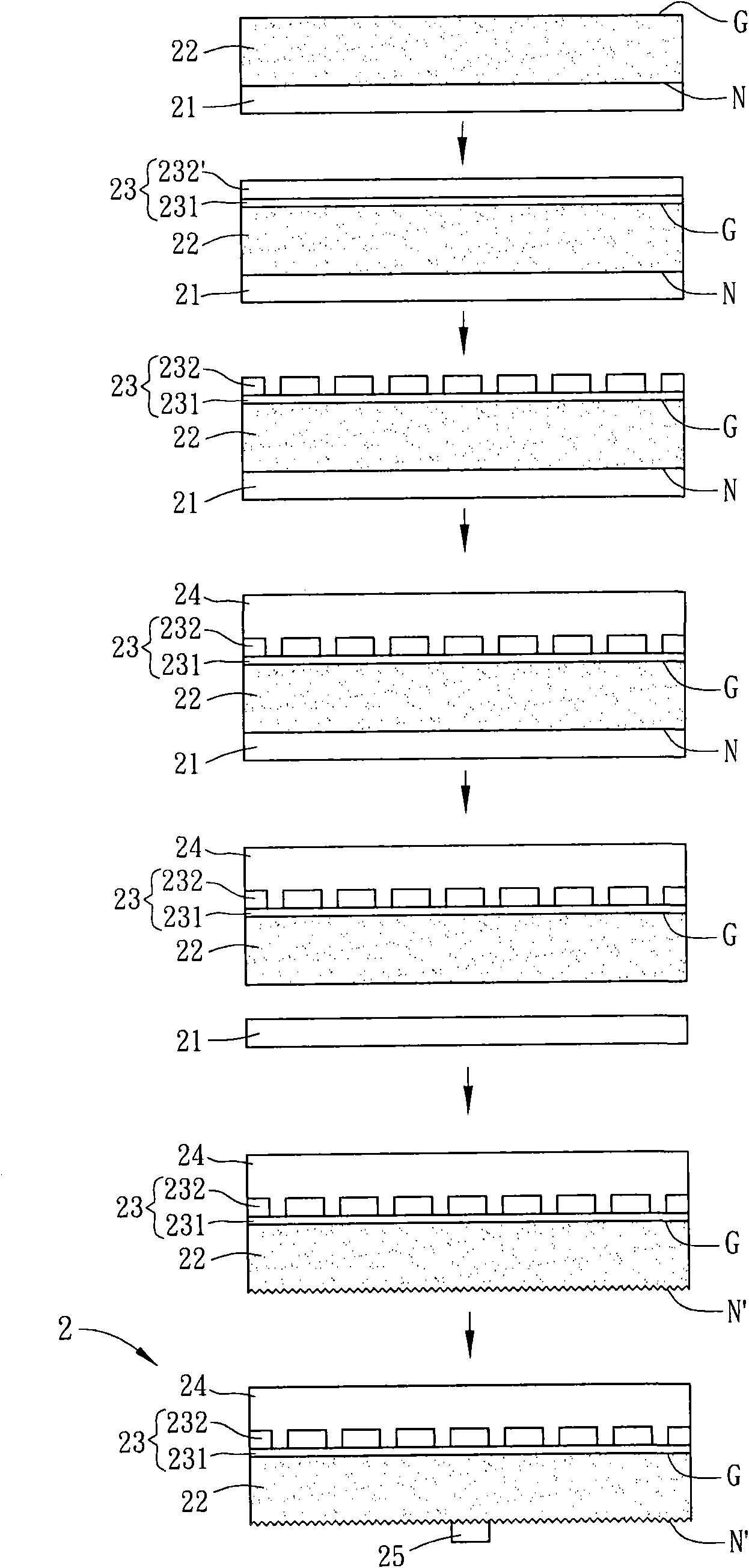
[0064] Please refer to Image 6 and Figure 7 As shown, a method for manufacturing an optoelectronic device according to the third embodiment of the present invention includes steps S31 to S37.
[0065] In step S31 , a photoelectric element 42 is formed on a substrate 41 . Wherein, the optoelectronic element 42 has a nitrogen polarity side N and a gallium polarity side G after formation, and in this embodiment, the nitrogen polarity side N is farther away from the substrate 41 than the gallium polarity side.
[0066] Different from the previous embodiments, in step S32 , before forming the reflective ohmic contact film 43 on the photoelectric element 42 , the nitrogen side N′ of the photoelectric element 42 is etched to roughen the nitrogen side N′. The reflective ohmic contact film 43 is formed in step S33 to step S36 of the process / treatment of the photoelectric element 42 respectively the same as step S12 to step S15 in the above-mentioned first embodiment. In this embod...
PUM
| Property | Measurement | Unit |
|---|---|---|
| thickness | aaaaa | aaaaa |
Abstract
Description
Claims
Application Information
 - R&D
- Intellectual Property
- Life Sciences
- Materials
- Tech Scout
- Unparalleled Data Quality
- Higher Quality Content
- 60% Fewer Hallucinations
Browse by: Latest US Patents, China's latest patents, Technical Efficacy Thesaurus, Application Domain, Technology Topic, Popular Technical Reports.
© 2025 PatSnap. All rights reserved.Legal|Privacy policy|Modern Slavery Act Transparency Statement|Sitemap|About US| Contact US: help@patsnap.com