
Photoresist burr edge-forming method and TFT-LCD array substrate-manufacturing method

An array substrate and photoresist technology, which is applied in semiconductor/solid-state device manufacturing, optics, optomechanical equipment, etc., can solve the problem that the three-time mask process cannot guarantee the quality of the lift-off process, and achieve the effect of wide applicability

Inactive Publication Date: 2010-01-20
BOE TECH GRP CO LTD +1
View PDF0 Cites 26 Cited by
  • Summary
  • Abstract
  • Description
  • Claims
  • Application Information

AI Technical Summary

Problems solved by technology

[0004] The purpose of the present invention is to provide a photoresist burr edge forming method and a TFT-LCD array substrate manufacturing method, which can effectively solve the technical defects such as the existing three-time mask process cannot guarantee the quality of the lift-off process

Method used


Image

  • Photoresist burr edge-forming method and TFT-LCD array substrate-manufacturing method
  • Photoresist burr edge-forming method and TFT-LCD array substrate-manufacturing method
  • Photoresist burr edge-forming method and TFT-LCD array substrate-manufacturing method

Examples


Embodiment Construction

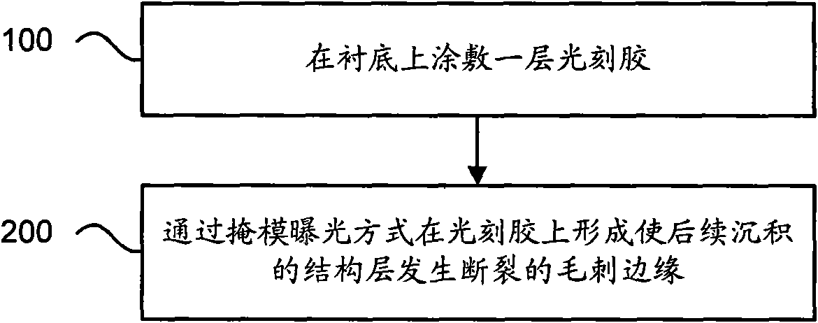
[0058] figure 1 It is a flow chart of the method for forming photoresist burr edges of the present invention, specifically including:

[0059] Step 100, coating a layer of photoresist on the substrate;

[0060] Step 200 , forming burr edges on the photoresist by mask exposure to break the subsequently deposited structural layer.

[0061] In the above technical scheme of the present invention, the substrate represents the formed structural pattern, such as the data line, source electrode, drain electrode and TFT channel area pattern that have been formed on the substrate. The burr edges can cause fractures in the subsequently deposited structural layers. Taking the preparation of the pixel electrode pattern as an example, when a transparent conductive film is deposited on the photoresist, due to the existence of the burr edge on the photoresist, the deposited transparent conductive film breaks at the raised structure of the burr edge, that is, the burr edge The transparent c...


PUM

PropertyMeasurementUnit
visible light transmittanceaaaaaaaaaa

Abstract

The invention relates to a photoresist burr edge-forming method and a TFT-LCD array substrate-manufacturing method. The TFT-LCD array substrate-manufacturing method comprises: forming a gate line and a gate electrode graph on a substrate; forming a data wire, a source electrode, a drain electrode and a TFT channel region, reserving photoresist, depositing a passivation layer and removing the photoresist together with the passivation layer on the photoresist through a lift-off stripping process; and smearing the photoresist, forming peak-shaped burr edges on the photoresist, depositing a transparent conductive film, forming a pixel electrode graph through the lift-off stripping process and directly connecting a pixel electrode with the drain electrode. The invention forms the photoresist burr edges through a third composition process and breaks the deposited transparent conductive film on the burr edges so as to effectively guarantee the quality of the lift-off stripping process, and has the advantages of simple reliable manufacturing process, easy implementation in practical production and broad application prospects.

Description

technical field [0001] The invention relates to the technical field of liquid crystal display manufacture, in particular to a photoresist burr edge forming method and a TFT-LCD array substrate manufacturing method. Background technique [0002] Thin Film Transistor Liquid Crystal Display (TFT-LCD for short) has the characteristics of small size, low power consumption, and no radiation, and occupies a dominant position in the current flat panel display market. For TFT-LCD, the array substrate and manufacturing process determine its product performance, yield and price. In order to effectively reduce the price of TFT-LCD and increase the yield, the manufacturing process of TFT-LCD array substrates has been gradually simplified, from the initial seven-mask process to four-mask based on slit lithography. Mode (4mask) process, the current three mask (3Mask) process is in the research stage. [0003] The prior art proposes a three-time mask (3Mask) process. First, the first comm...

Claims


Application Information

Patent Timeline
Patent Type & Authority Applications(China)
IPC IPC(8): H01L21/027H01L21/321H01L21/768H01L21/28H01L21/84H01L27/12H01L23/522G03F7/42G03F7/36G03F7/26G02F1/1362
CPCH01L27/1288G03F1/144H01L21/0274H01L21/0272H01L27/1214G03F1/00G03F7/2022G03F1/36
Inventor 郑云友郑载润侯智刘祖宏李正勲
Owner BOE TECH GRP CO LTD
Learn More