Technique for atomic layer deposition

An atomic layer and atomic technology, applied in coating, metal material coating process, gaseous chemical plating, etc., can solve problems such as difficult to achieve dopant uniformity, damage, film compliance doping, etc.

Inactive Publication Date: 2010-01-20
VARIAN SEMICON EQUIP ASSOC INC
View PDF0 Cites 27 Cited by
  • Summary
  • Abstract
  • Description
  • Claims
  • Application Information

AI Technical Summary

Problems solved by technology

Further, energetic ions also cause crystalline defects, which necessitates post-deposition annealing
[0006] Moreover, conformal doping of ALD-deposited films, especially in 3-D structures (e.g., FinFETs), remains a challenge for process engineers
It is not desirable to use existing ion implantation techniques to introduce dopants into a 3-D conformally covered structure, not only because it is difficult to achieve uniform dopant distribution, but also because the implantation Potential damage from post-implant anneal

Method used


Image

  • Technique for atomic layer deposition
  • Technique for atomic layer deposition
  • Technique for atomic layer deposition

Examples


Embodiment Construction

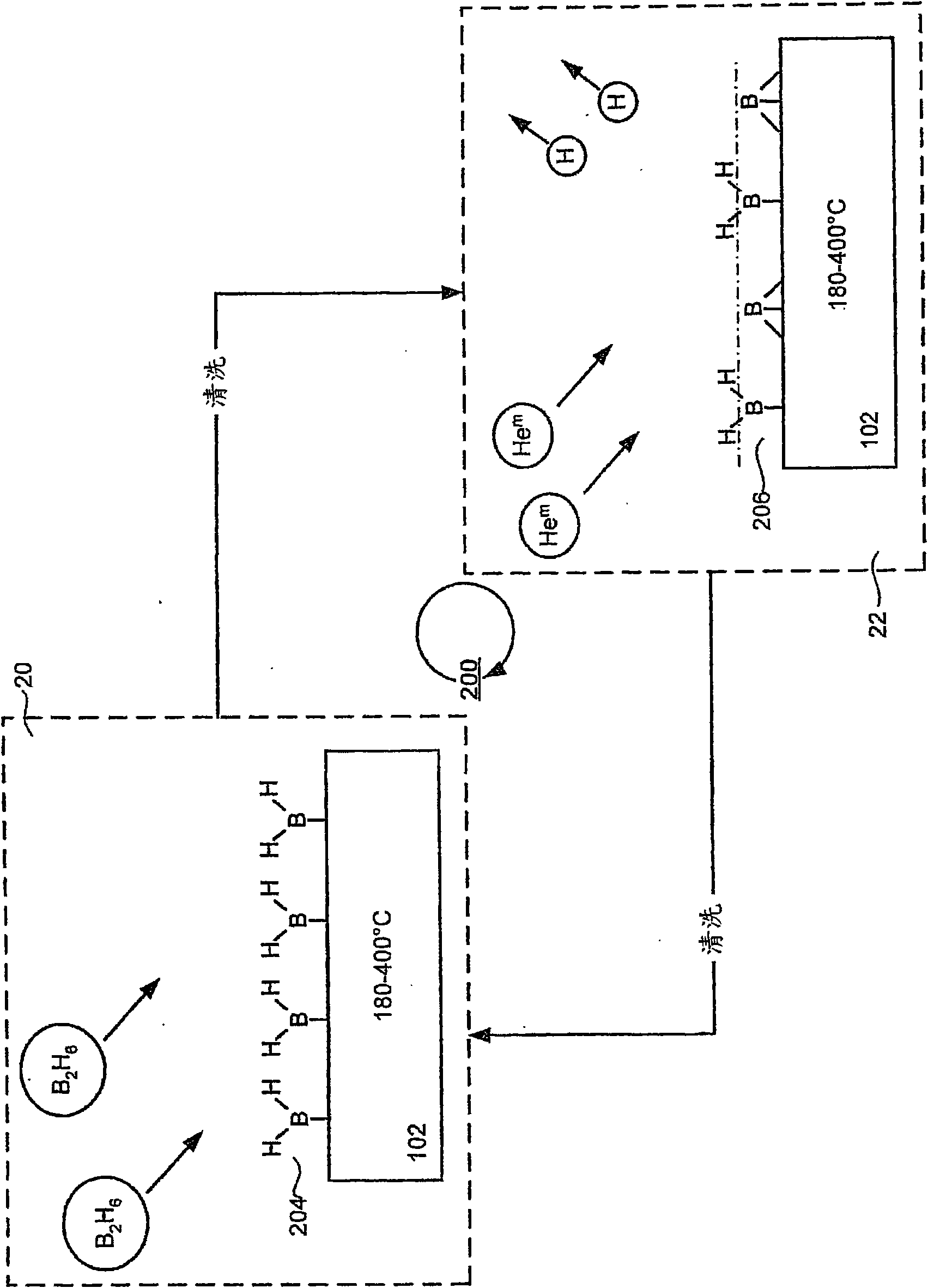
[0017] In order to solve the above-mentioned technical problems related to the existing atomic layer deposition technology, embodiments of the present invention introduce ALD and in situ doping technology. Use metastable atoms to desorb excess atoms. For example, metastable atoms are generated within the plasma chamber. For purposes of illustration, the ensuing description will focus on methods and apparatus for depositing doped or undoped silicon using helium metastable atoms. It will be appreciated that films of other species can also be grown using the same or similar techniques using helium or other metastable atoms.

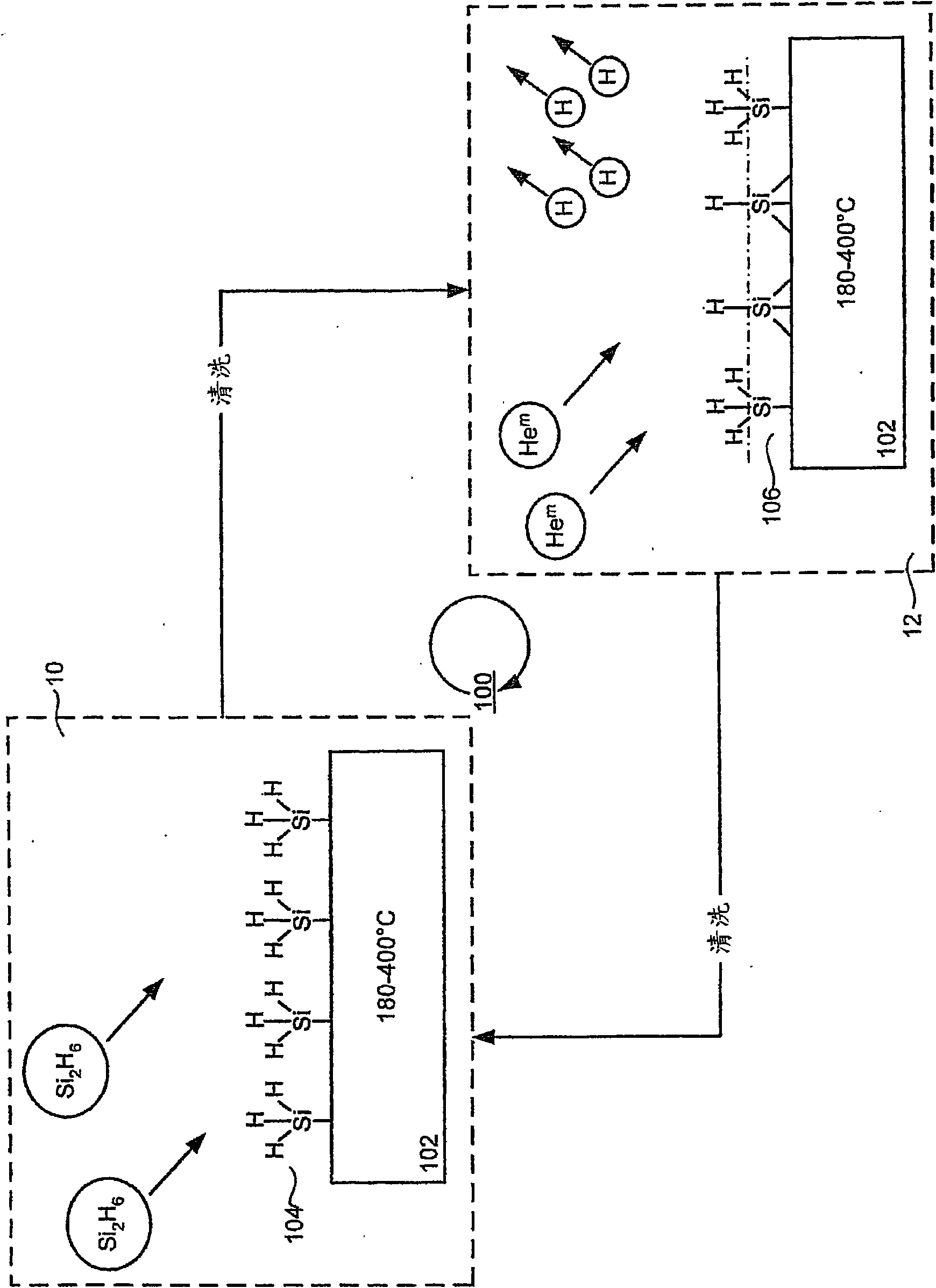
[0018] refer to figure 1 , which shows a schematic block diagram of an atomic layer deposition cycle 100 according to an embodiment of the present invention. The atomic layer deposition cycle 100 includes two phases, a saturation phase 10 and a desorption phase 12 .

[0019] In the saturation phase 10, the substrate 102 is exposed to disilane (Si2H6) gas...


PUM


Abstract

A technique for atomic layer deposition is disclosed. In one particular exemplary embodiment, the technique may be realized by a method for forming a strained thin film. The method may comprise supplying a substrate surface with one or more precursor substances having atoms of at least one first species and atoms of at least one second species, thereby forming a layer of the precursor substance on the substrate surface. The method may also comprise exposing the substrate surface to plasma-generated metastable atoms of a third species, wherein the metastable atoms desorb the atoms of the at least one second species from the substrate surface to form an atomic layer of the at least one first species. A desired amount of stress in the atomic layer of the at least one first species may be achieved by controlling one or more parameters in the atomic layer deposition process.

Description

technical field [0001] The present invention relates to semiconductor technology, in particular to atomic layer deposition (atomic layer deposition) technology. Background technique [0002] Modern semiconductor processing has created a need for precise atomic-level deposition of high quality thin film structures. In response to this need, various film growth techniques collectively referred to as "atomic layer deposition (ALD)" or "atomic layer epitaxy (ALE)" have been developed in recent years. ALD techniques are capable of depositing uniform and conformable films with atomic layer accuracy. Typical ALD processes use continuous self-limiting surface reactions to control film growth within a monolayer thickness regime. Due to its good potential for film conformity and uniformity, ALD has become the technology of choice for advanced applications such as high-k gate oxides in microelectronic assemblies, storage capacitor dielectrics, and Copper diffusion barrier. In fact,...

Claims


Application Information

Patent Timeline
Patent Type & Authority Applications(China)
IPC IPC(8): C23C16/455H01L21/00
CPCC23C16/4554H01L21/32155H01L21/3185C23C16/22C23C16/452C23C16/345H01L21/3141H01L21/02274H01L21/0228H01L21/0217C23C16/34C23C16/45525H01L21/0262
Inventor 维克拉姆·辛哈勒德·M·波辛艾德蒙德·J·温德安东尼·雷诺乔治·D·帕帕守尔艾迪斯
Owner VARIAN SEMICON EQUIP ASSOC INC
Why Eureka
Try Eureka