

Inductive coupling coil and plasma processing device adopting same
An inductively coupled coil and coil winding technology, applied in the field of microelectronics, can solve the problems of slow processing of the central part of the wafer processing/processing process, uneven processing/processing results, and difficulty in obtaining plasma, and achieve uniform processing/processing results. The effect of uniform plasma density distribution and easy conjugate matching
- Summary
- Abstract
- Description
- Claims
- Application Information
AI Technical Summary
Problems solved by technology
Method used
Image

Examples
Embodiment Construction
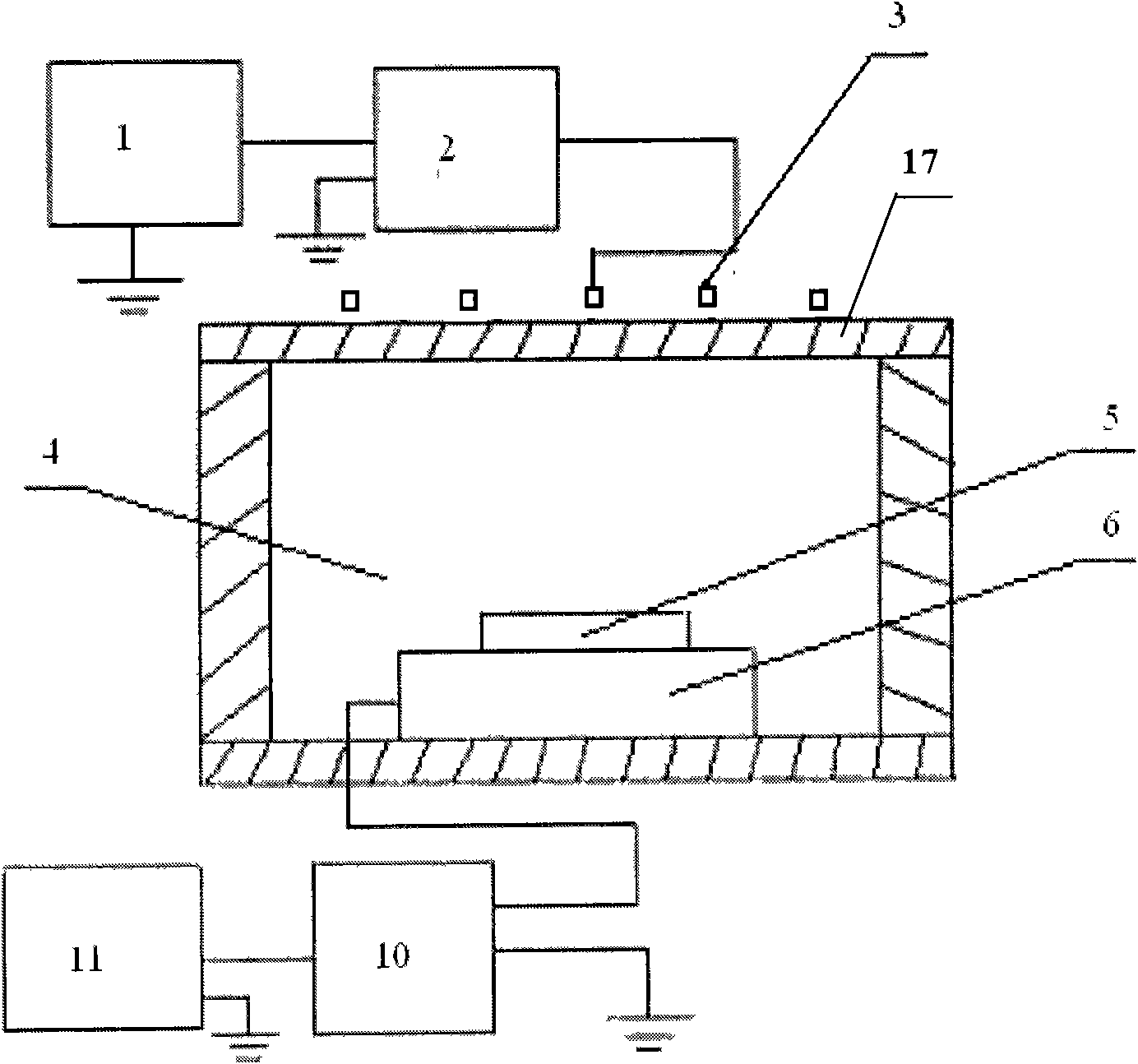
[0043] In order to enable those skilled in the art to better understand the technical solution of the present invention, the inductively coupled coil and the plasma processing device using the inductively coupled coil provided by the present invention will be described in detail below with reference to the accompanying drawings.
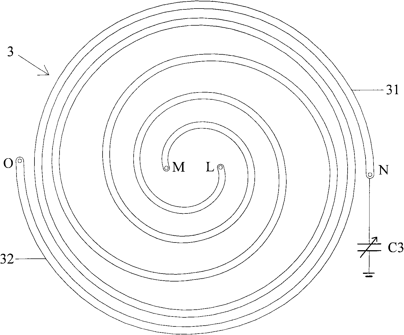
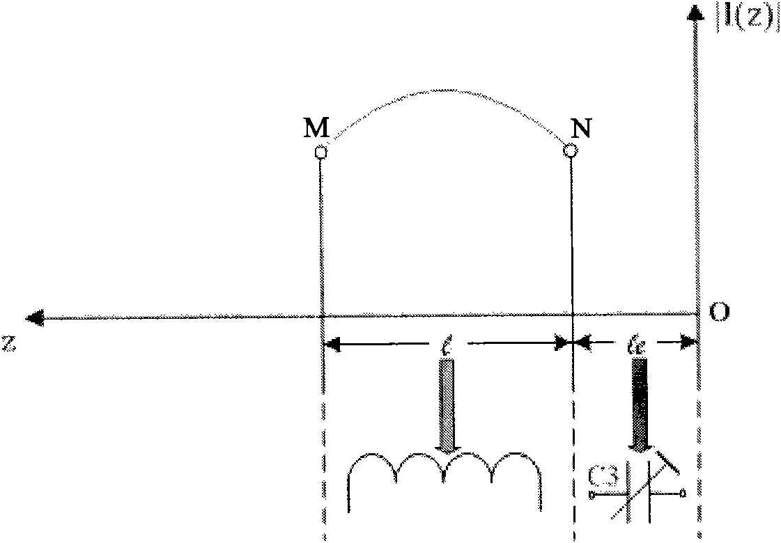
[0044] see Figure 4 The inductively coupled coil 4 provided by the first embodiment of the present invention includes two identical spiral coil windings (that is, the first winding 41 and the second winding 42) that are parallel to each other and nested in each other, each of which is helical The linear coil windings are all planar structures. The input end of the first winding 41 is a, the output end is d; the input end of the second winding 42 is c, and the output end is b. The input end a of the first winding 41 is connected to the matching device, and the input end c of the second winding 42 is connected to the matching device; the output end d...
PUM
| Property | Measurement | Unit |
|---|---|---|
| size | aaaaa | aaaaa |
Abstract
Description
Claims
Application Information