Epitaxial method for preparing AlGaAsSb/InGaAsSb multi-quantum wells by using AlSb buffer layer

A multi-quantum well and multi-quantum well layer technology is applied in the field of epitaxial growth of semiconductor laser materials and new semiconductor laser materials. It can solve the problems of high-quality material growth difficulty, antimonide material and device difficulty, etc., to improve quality and increase The effect of material properties

Inactive Publication Date: 2010-02-10
CHANGCHUN UNIV OF SCI & TECH
View PDF0 Cites 8 Cited by
  • Summary
  • Abstract
  • Description
  • Claims
  • Application Information

AI Technical Summary

Problems solved by technology

However, the research on antimonide materials and devices is quite difficult. Antimonide materials have a large immiscible gap, and the materials in the immiscible gap are metasta

Method used


Image

  • Epitaxial method for preparing AlGaAsSb/InGaAsSb multi-quantum wells by using AlSb buffer layer
  • Epitaxial method for preparing AlGaAsSb/InGaAsSb multi-quantum wells by using AlSb buffer layer
  • Epitaxial method for preparing AlGaAsSb/InGaAsSb multi-quantum wells by using AlSb buffer layer

Examples


Embodiment Construction

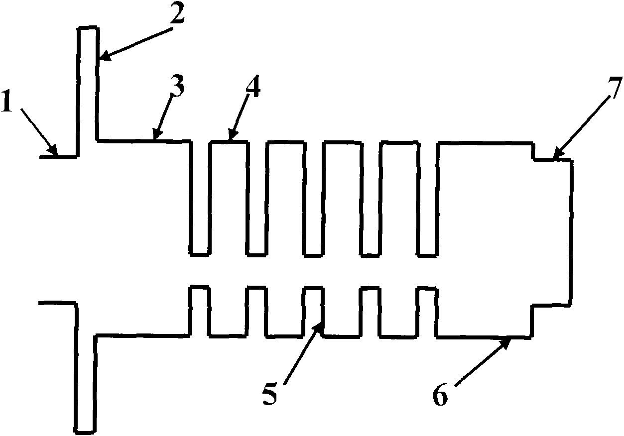
[0009] Such as figure 1 As shown, the structure of the AlGaAsSb / InGaAsSb multiple quantum well prepared by the AlSb buffer layer includes: n-type GaSb substrate (1); AlSb buffer layer (2); n-type Al 0.35 Ga 0.65 As 0.03 Sb 0.97 Lower confinement layer (3); 5 cycles of Al 0.35 Ga 0.65 As 0.03 Sb 0.97 / In 0.65 Ga 0.35 As 0.1 Sb 0.9 Multiple quantum well layer (4) / (5); p-type Al 0.35 Ga 0.65 As 0.03 Sb 0.97 Upper confinement layer (6); p-type GaSb ohmic layer (7).

[0010] In the following, the present invention will be explained with examples, and the equipment used is molecular beam epitaxy equipment (MBE).

[0011] On GaSb substrate (1), Te doping concentration is 1~2×10 17 cm -3 The GaSb crystal material grows sequentially;

[0012] AlSb buffer layer (2), the growth temperature is 500℃, and the thickness is 30nm;

[0013] Al 0.35 Ga 0.65 As 0.03 Sb 0.97 Lower confinement layer (3), growth temperature 520℃, Te doping, concentration 5×10 18 cm -3 , Grow 0.3μm;

[0014] 5 cycles of 15nm-A...


PUM

PropertyMeasurementUnit
Thicknessaaaaaaaaaa
Thicknessaaaaaaaaaa

Abstract

An AlGaAsSb/InGaAsSb multi-quantum well laser belongs to first Class of quantum well structure, the materials and the devices are very difficult to research; large immiscible gaps exist in antimonidematerial, the material in the immiscible gaps is in the metastable state, the high-quality material is very difficult to grow, the material is one of the most complicated materials in Group III-V compounds and also one of the scientific key points mainly researched in the world. The invention provides an epitaxial method for preparing AlGaAsSb/InGaAsSb multi-quantum wells by using an AlSb buffer layer. The AlSb buffer layer can be used for obtaining high crystal quality and high surface flatness. The AlSb buffer layer can be used as a surfactant to reduce the interfacial free energy between the substrate and the epitaxial layer, and can also be used as a filter board to prevent dislocation from happening. The method is used for preparing materials of high-quality AlGaAsSb/InGaAsSb multi-quantum well laser.

Description

Technical field [0001] The invention relates to the technical field of semiconductor laser materials, and belongs to the technical field of epitaxial growth of new semiconductor laser materials. Background technique [0002] III-V compound semiconductor lasers mainly include GaN-based ultraviolet / near-ultraviolet lasers; visible light, near-infrared InP-based and GaAs-based multiple quantum well lasers; 2-5μm GaSb-based lasers and covering mid-infrared and far-infrared (THz) bands Quantum cascade laser (QCL), etc. Due to technical reasons and the rapid development of the information industry, research on GaAs-based and InP-based multi-quantum well lasers has been extensively carried out in the past, and its technology is now relatively mature. Lasers and detectors working in this band have important applications in many fields of military and civilian use. It has important applications in the fields of trace gas detection, industrial control, atmospheric environment monitoring,...

Claims


Application Information

Patent Timeline
IPC IPC(8): H01S5/343
Inventor 李占国刘国军尤明慧李林李梅乔忠良邹永刚邓昀王勇王晓华赵英杰
Owner CHANGCHUN UNIV OF SCI & TECH
Why Eureka
Try Eureka