Array piezoresistive tactile sensor adopting voltage array feedback method to weaken return circuit interference of scanning circuits

A tactile sensor and scanning circuit technology, applied in electrical components, coding, keyboard-like equipment coding, etc., can solve the problems of complex realization circuits, circuit interference of row and column scanning circuits, weakening circuit interference of scanning circuits, etc., and achieve accurate and complex results. reduced effect

Inactive Publication Date: 2010-04-14
HARBIN INST OF TECH
View PDF0 Cites 8 Cited by
  • Summary
  • Abstract
  • Description
  • Claims
  • Application Information

AI Technical Summary

Problems solved by technology

However, while reducing the external leads, the loop interference problem of the row-column scanning circuit is unavoidable.
The existing methods of eliminating loop interference include: using silicon technology to preprocess and integrate the tactile unit, integrating the integrated circuit with the sensor and connecting diodes in series. This method increases the production cost of the sensor and makes the tactile sensor lack of flexibility; There is a method of voltage feedback. This method feeds back the output voltage of the current scanning column to the non-current scanning row and non-current scanning column at the same time. Although it can effectively weaken the loop interference of the scanning circuit, it does not affect the compliance of the tactile sensor. However, the implementation circuit is very complicated, which affects the reliability of the entire system and the miniaturization of the processing circuit

Method used


Image

  • Array piezoresistive tactile sensor adopting voltage array feedback method to weaken return circuit interference of scanning circuits
  • Array piezoresistive tactile sensor adopting voltage array feedback method to weaken return circuit interference of scanning circuits
  • Array piezoresistive tactile sensor adopting voltage array feedback method to weaken return circuit interference of scanning circuits

Examples


specific Embodiment approach 1

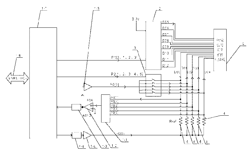
[0010] Specific embodiment one: the following combination figure 1 , image 3 Figure 9 Illustrating this embodiment, this embodiment includes a haptic signal acquisition flexible circuit board 5, which further includes a switch circuit 1-1, an amplifier circuit 1-2, an ADC circuit 1-3, a DAC circuit 1-4, and a first analog signal output register 1-5, the second analog signal output register 1-6, the logic control circuit 1-7, the multiplex switch 2, the analog switch 3 and a plurality of comparison resistors 4,

[0011] The reference low-voltage output terminal of the logic control circuit 1-7 is connected to the digital signal input terminal of the DAC circuit 1-4, and the analog signal output terminal of the DAC circuit 1-4 is connected to the analog signal input terminal of the second analog signal output register 1-6. Two analog signal output The analog signal output end of the registers 1-6 is connected to one end of each comparison resistor 4, and the other end of eac...

specific Embodiment approach 2

[0021] Embodiment 2: The difference between this embodiment and Embodiment 1 is that it also includes SPIM interface circuits 1-8, and the sampling signal input end of the SPIM interface circuit 1-8 is connected to the sampling signal output end of the logic control circuit 1-7 It is used for communication with the upper computer. Other components and connection relationships are the same as those in the first embodiment.

specific Embodiment approach 3

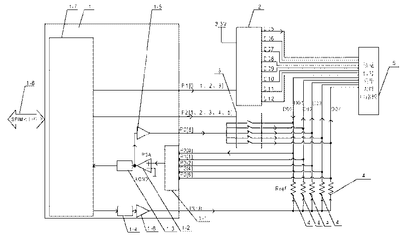
[0022] Specific embodiment three: the following combination figure 2 This embodiment will be described. The difference between this embodiment and Embodiment 2 is that the switch circuit 1-1, the amplifier circuit 1-2, the ADC circuit 1-3, the DAC circuit 1-4, and the first analog signal output register 1 -5. The second analog signal output register 1-6, the logic control circuit 1-7 and the SPIM interface circuit 1-8 are integrated in the PSoC mixed-signal array programmable system-on-chip 1. Other compositions and connection relationships are the same as those in the second embodiment.

[0023] In this embodiment, the PSoC mixed-signal array programmable system-on-a-chip 1 is used as the main processing chip. Through the voltage column feedback method, the circuit structure is simplified while the circuit interference of the tactile sensor scanning circuit is effectively weakened, and the functions of some peripheral circuits are integrated. In the main processing chip, th...


PUM


Abstract

An array piezoresistive tactile sensor adopting voltage array feedback method to weaken return circuit interference of scanning circuits belongs to the field of array piezoresistive tactile sensors. The sensor solves the problem of a return circuit interference of a scanning circuit in the array piezoresistive tactile sensor, simultaneously realizes the more simple circuit. The sensor weakens thereturn circuit interference of the line scanning circuit of the array piezoresistive tactile sensor after transferring output voltage signals of the current scanning line on a signal collecting flexible circuit board to a switch circuit and an amplifier circuit, namely the signals are divided into two paths, one path of the signals are converted into the digital quantity through an ADC circuit, thereby realizing collecting the tactile sense information, the other path of the signals are fed back into non-sampling array electrodes through a first analog signal output storage and analog switch,and a logical control circuit controls a multiway switch to provide standard high voltage for the current scanning line on the tactile sense signal collecting flexible circuit board. The array piezoresistive tactile sensor can effectively weaken the return circuit interference of scanning circuits.

Description

technical field [0001] The invention relates to an array piezoresistive tactile sensor which adopts a voltage column feedback method to weaken the interference of a scanning circuit loop, belonging to an array piezoresistive tactile sensor. Background technique [0002] The existing array piezoresistive tactile sensor adopts the form of row and column scanning to collect signals, which can effectively reduce the number of external leads of the tactile sensor. However, while reducing the external leads, the loop interference problem of the row-column scanning circuit is inevitably generated. The existing methods for eliminating loop interference include: using silicon technology to preprocess and integrate the tactile unit, integrating the integrated circuit and the sensor and connecting diodes in series, this method increases the cost of sensor fabrication and makes the tactile sensor lack flexibility; There is a method of voltage feedback. This method feeds back the output...

Claims


Application Information

Patent Timeline
Patent Type & Authority Applications(China)
IPC IPC(8): H03M11/00
Inventor 张元飞刘宏刘伊威金明河吴克
Owner HARBIN INST OF TECH
Why Eureka
Try Eureka