
Single-lens multi-angle high-magnification photonic chip coupling and packaging device

A photonic chip and packaging device technology, applied in the fields of optoelectronics and integrated optics, can solve the problems of large size, increased cost, unfavorable coupling alignment, etc., and achieves high linear displacement accuracy and angular displacement accuracy, and good consistency.

Inactive Publication Date: 2010-04-21
SOUTHEAST UNIV
View PDF0 Cites 12 Cited by
  • Summary
  • Abstract
  • Description
  • Claims
  • Application Information

AI Technical Summary

Problems solved by technology

The imaging system is divided into two channels of observation, which makes the system architecture complex, large, and costly, and it is impossible to obtain all-round images of objects from other angles, which is not conducive to accurate coupling alignment

Method used


Image

  • Single-lens multi-angle high-magnification photonic chip coupling and packaging device
  • Single-lens multi-angle high-magnification photonic chip coupling and packaging device
  • Single-lens multi-angle high-magnification photonic chip coupling and packaging device

Examples


specific Embodiment approach

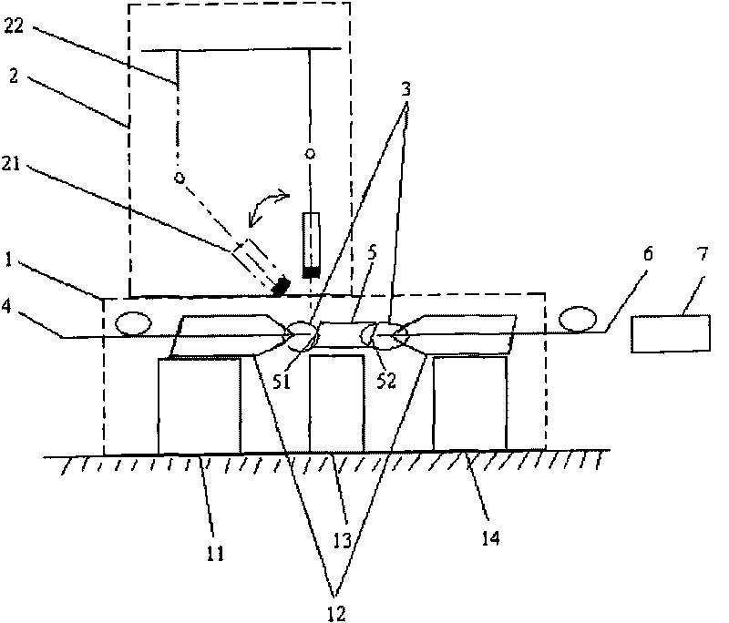
[0046] figure 1 It is a structural representation of the present invention. The coupling adjustment device 1 is composed of a six-dimensional fine-tuning frame 11 , a V-shaped groove 12 , a chip platform 13 and a three-dimensional fine-tuning frame 14 . The machine vision device 2 is composed of a lens camera assembly 21 and a multi-angle fixed swivel device 22 . The optical fiber-chip curing device 3 is an ultraviolet glue curing device using a UV-LED light source. Its specific implementation is as follows:

[0047] ① Fix the chip 5 on the chip platform 13 . Under the observation and guidance of the machine vision device 2, use the three-dimensional fine-tuning frame 14 to manually roughly adjust the output fiber 6 located on the V-shaped groove 12, align with the output end 52 of the chip 5, and lock the three-dimensional fine-tuning frame 14; adjust the lens by fixing the rotary device 22 The camera assembly 21 observes the incident end 51 of the chip 5 , uses the six-d...

Embodiment 2

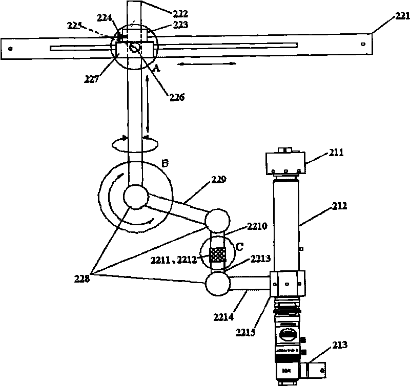
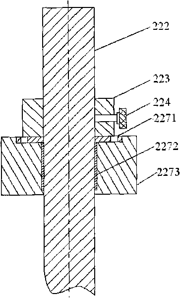
[0051] figure 2 is in the present invention figure 1 The assembly schematic diagram of the core part machine vision device 2 shown. The lens camera assembly 21 is composed of a lens 211 , a camera 212 , and a point light source 213 . The multi-angle fixed swing device 22 consists of a crossbeam 221, a main rod 222, a sliding sleeve 223, a bolt 224, a horizontal fastening bolt 225, a vertical fastening bolt 226, a connecting sliding sleeve 227, a swing adjustment handwheel 228, a first connecting rod 229, The upper connecting rod 2210, the joint 2211, the connecting sleeve 2212, the lower connecting rod 2213, the second connecting rod 2214, and the lens clamp 2215 are composed. Connecting sliding sleeve 227 is made of rod sleeve bottom ring 2271, bushing 2272, main rod sleeve 2273.

[0052] Its specific implementation is as follows:

[0053] ① The vertical adjustment assembly is composed of a main rod 222, a sliding sleeve 223, a bolt 224 and a vertical fastening bolt 226....


PUM


Abstract

The invention discloses a single-lens multi-angle high-magnification photonic chip coupling and packaging device which comprises a coupling adjusting device, a machine vision device and an optical-chip curing device, wherein the machine vision device comprises a lens camera assembly and a multi-angle fixing gyroscope, the lens camera assembly is arranged on the multi-angle fixing gyroscope and comprises a high-magnification lens with optical magnification of 3.5-22.5X and a high-sensitivity CMOS camera, and the high-magnification lens is arranged on the CMOS camera. By the total magnification of 175-1125X of imaging of a CMOS chip in a display, the single-lens multi-angle high-magnification photonic chip coupling and packaging device can realize 180-degree rotation under the self-designed fixing gyroscope and observation of submicron and nanometer wave guide light paths at any angle of nearly 90 degrees from vertical overlooking to horizontal side-looking, wherein an image can not shake.

Description

1. Technical field [0001] The invention belongs to the technical field of optoelectronics and integrated optics, and relates to a photonic chip coupling and packaging device used in industrial sites, laboratories, etc. Photonic chip coupling and packaging systems for micron and nanoscale photonic chips and optical fiber coupling, alignment, and packaging purposes. 2. Technical Background [0002] As photonic chip technology gradually matures, packaging technology must be given full attention, and the requirements for the alignment and coupling of photonic chips and optical fibers are also getting higher and higher. The core diameter of ordinary single-mode optical fiber is about 8 microns, and the waveguide width of photonic chips varies with materials. The chip waveguide width is on the order of submicron. Realizing precise alignment and efficient coupling between photonic chips and optical fibers requires nanoscale six-dimensional fine-tuning technology (longitudinal, la...

Claims


Application Information

Patent Timeline
Patent Type & Authority Applications(China)
IPC IPC(8): G02B6/24
Inventor 孙小菡刘旭蒋卫锋
Owner SOUTHEAST UNIV
Learn More