Catch for etching process and method for preventing catch from jumping

A technology of baffle and process, which is applied in the direction of electrical components, semiconductor/solid-state device manufacturing, circuits, etc., can solve the problems of baffle jumping, affecting mass production efficiency, and baffle self-alignment failure, etc., to reduce the strength , low cost, and the effect of increasing weight

Active Publication Date: 2010-04-21
SHANGHAI HUAHONG GRACE SEMICON MFG CORP
View PDF0 Cites 2 Cited by
  • Summary
  • Abstract
  • Description
  • Claims
  • Application Information

AI Technical Summary

Problems solved by technology

Since each etching will reduce the thickness of the warm-up film on the wafer surface, after the 8th etching, the warm-up film on the wafer surface has been etched, and the DC bias voltage decreases rapidly, so frequent b

Method used


Image

  • Catch for etching process and method for preventing catch from jumping
  • Catch for etching process and method for preventing catch from jumping
  • Catch for etching process and method for preventing catch from jumping

Examples


Embodiment Construction

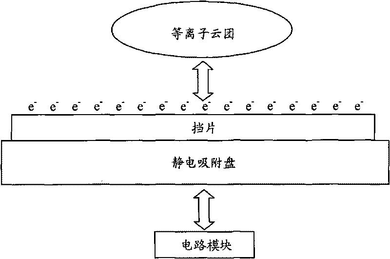
[0012] In order to reduce the probability of chip jumping in the etching process, the present invention proposes the following physical model to explain the process of chip jumping and propose a solution:

[0013] 1. Chip jumping occurs when the electrostatic adsorption disc discharges electrons on the wafer surface;

[0014] 2. During the process of electronic discharge on the surface of the wafer, the wafer will vibrate, and the faster the discharge speed, the stronger the vibration;

[0015] 3. The speed of discharge is related to the equivalent resistance of the block, the greater the resistance, the slower the discharge speed;

[0016] 4. Increasing the weight of the baffle can reduce the intensity of the vibration.

[0017] Based on the above physical model, the solution principle of the present invention is: to increase the equivalent resistance of the baffle, so as to weaken the vibration of the baffle during discharge, thereby reducing the probability of chip jumping...


PUM

PropertyMeasurementUnit
Thicknessaaaaaaaaaa
Resistivityaaaaaaaaaa

Abstract

The invention discloses a catch for an etching process, comprising a wafer substrate and a warming film layer arranged on the wafer substrate and an insulated film layer for preventing the jumping is arranged below the wafer substrate. The invention also discloses a method for preventing the catch from jumping, comprising the step that an insulated film layer for preventing the jumping is grown at the bottom of the wafer substrate of the catch. The invention has the advantages that equivalent resistance of the catch can be increased so as to weaken the vibration of the catch during discharge, thereby the jumping probability can be reduced; the insulated film layer is added and further the weight of the catch can be increased, thus the intensity for vibration can be reduced; in addition, the insulated layer can be repeatedly used and has the advantage of low cost.

Description

technical field [0001] The invention relates to a baffle used in the etching process, and also relates to a method for preventing the baffle from jumping in the etching process. Background technique [0002] Such as figure 1 As shown, in the semiconductor etching process, in order to reduce the impact of the accumulation of polymer in the etching reaction chamber on the etching process, before etching, a block is used to warm up. The high-voltage circuit of the circuit module can make the electrostatic adsorption disc absorb the block (wafer) during the etching process, and release the electrons on the surface of the wafer after the etching process is completed. + . The steps for repeatability testing of the baffle are: the baffle enters the main etching reaction chamber to warm up; the baffle enters the self-alignment chamber for self-alignment; the baffle enters the main etching reaction chamber to warm up... so repeatedly. [0003] Such as figure 2 As shown, curve 1...

Claims


Application Information

Patent Timeline
IPC IPC(8): H01L21/00H01L21/316H01L21/66
Inventor 夏军殷冠华许昕睿林俊毅
Owner SHANGHAI HUAHONG GRACE SEMICON MFG CORP
Why Eureka
Try Eureka