

Washing method of monocrystalline/polycrystalline silicon chips
A technique for polycrystalline silicon wafers and silicon wafers, applied in liquid cleaning methods, cleaning methods and utensils, chemical instruments and methods, etc., which can solve problems such as environmental pollution and increased production costs
- Summary
- Abstract
- Description
- Claims
- Application Information
AI Technical Summary
Problems solved by technology
Method used
Image

Examples
Embodiment 1
[0039] Embodiment 1, a kind of cleaning method of monocrystalline / polycrystalline silicon chip, carries out following steps successively:
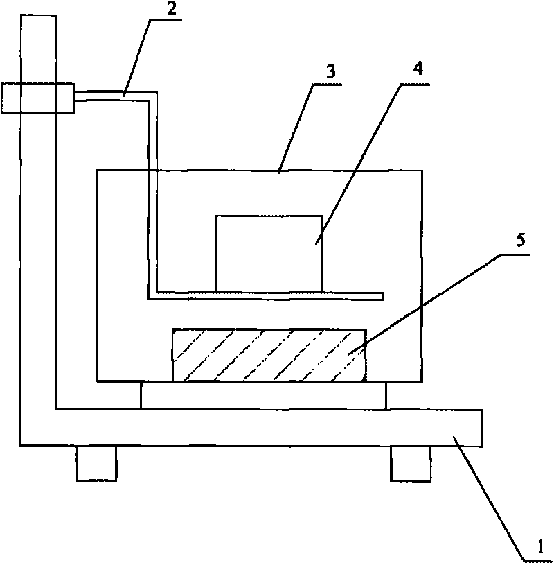
[0040] Each of the following steps 1) to 6) uses a specific cleaning tank, that is, step 1) uses 1# cleaning tank, step 2) uses 2# cleaning tank, step 3) uses 3# cleaning tank, and step 4 ) use 4# cleaning tank, step 5) use 5# cleaning tank, and step 6) use 6# cleaning tank.
[0041] The volumes of the 1# cleaning tank to the 6# cleaning tank are all 45L.
[0042] 1), Rough cleaning (using 1# cleaning tank):
[0043] Insert the ground silicon wafers into the PFA flower basket first. The PFA flower basket can be the 25-piece PFA flower basket produced by entergrits. Then put the PFA flower basket loaded with silicon wafers into the washing basket 4 of the 1# cleaning tank, and deionized water is housed in the tank body 3 of the 1# cleaning tank. The entire PFA flower basket is immersed in deionized water, and the up and down shaking freq...
Embodiment 2
[0061] Embodiment 2, a kind of cleaning method of monocrystalline / polycrystalline silicon chip, carries out following steps successively:
[0062] 1), Rough cleaning (using 1# cleaning tank):
[0063] Change the up and down shaking frequency of the rocking arm 2 to 90 times / minute, and the ultrasonic frequency to 20KHz; change the rough cleaning time to 20 minutes, and the rest are the same as in Example 1.
[0064] 2), soaking (using 2# cleaning tank):
[0065] Concentration is housed in the tank body 3 of this 2# cleaning tank and is the KOH solution of 5%, and soaking time is 2 minutes. All the other are with embodiment 1.
[0066] 3), cleaning (using 3# cleaning tank):
[0067] Set the up and down shaking frequency of the rocking arm 2 to 80 times / minute, the ultrasonic frequency to 20KHz; the cleaning time to 20 minutes; the rest are the same as in Example 1.
[0068] 4), alkali washing (using 4# cleaning tank):
[0069] The tank body 3 of this 4# cleaning tank is eq...
Embodiment 3
[0078] Embodiment 3, a kind of cleaning method of monocrystalline / polycrystalline silicon chip, carries out following steps successively:
[0079] 1), Rough cleaning (using 1# cleaning tank):
[0080] Change the up and down shaking frequency of the rocking arm 2 to 90 times / minute, change the ultrasonic frequency to 100KHz; change the rough cleaning time to 2 minutes, and the rest are the same as in Example 1.
[0081] 2), soaking (using 2# cleaning tank):
[0082] Concentration is housed in the tank body 3 of this 2# cleaning tank and is the KOH solution of 3%, and soaking time is 15 minutes. All the other are with embodiment 1.
[0083] 3), cleaning (using 3# cleaning tank):
[0084] Set the up and down shaking frequency of the rocking arm 2 to 80 times / minute, the ultrasonic frequency to 100KHz; the cleaning time to 2 minutes; the rest are the same as in Example 1.
[0085] 4), alkali washing (using 4# cleaning tank):
[0086] The tank body 3 of this 4# cleaning tank i...
PUM
| Property | Measurement | Unit |
|---|---|---|
| The average thickness | aaaaa | aaaaa |
Abstract
Description
Claims
Application Information