Method for manufacturing oxide layer capable of reducing gradient of side wall

A manufacturing method and oxide layer technology, applied in semiconductor/solid-state device manufacturing, electrical components, circuits, etc., can solve problems affecting device performance, etc., achieve the effect of increasing the etching speed and reducing the slope of the side wall

Active Publication Date: 2010-06-02
SHANGHAI HUAHONG GRACE SEMICON MFG CORP
View PDF0 Cites 11 Cited by
  • Summary
  • Abstract
  • Description
  • Claims
  • Application Information

AI Technical Summary

Problems solved by technology

When the field oxide layer is manufactured, the slope of the side wall is an important parameter. When the slope of the side wall is large, for example, when the angle between it and the silicon substrate

Method used


Image

  • Method for manufacturing oxide layer capable of reducing gradient of side wall
  • Method for manufacturing oxide layer capable of reducing gradient of side wall
  • Method for manufacturing oxide layer capable of reducing gradient of side wall

Examples


Embodiment Construction

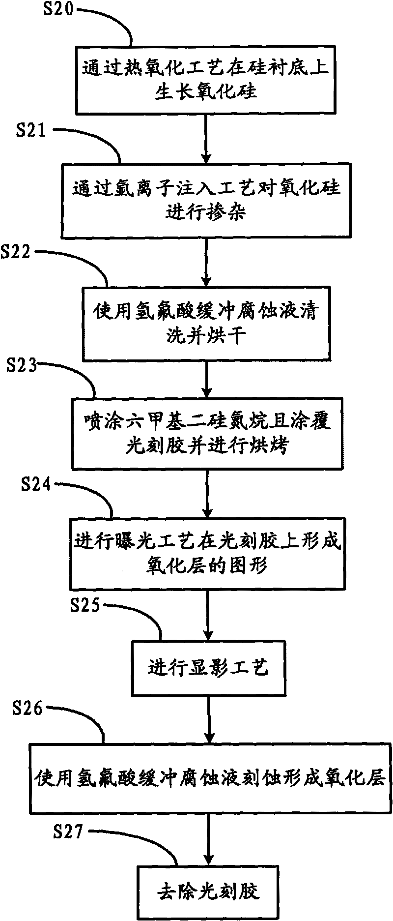
[0022] The oxide layer manufacturing method capable of reducing the slope of the sidewall of the present invention will be further described in detail below.

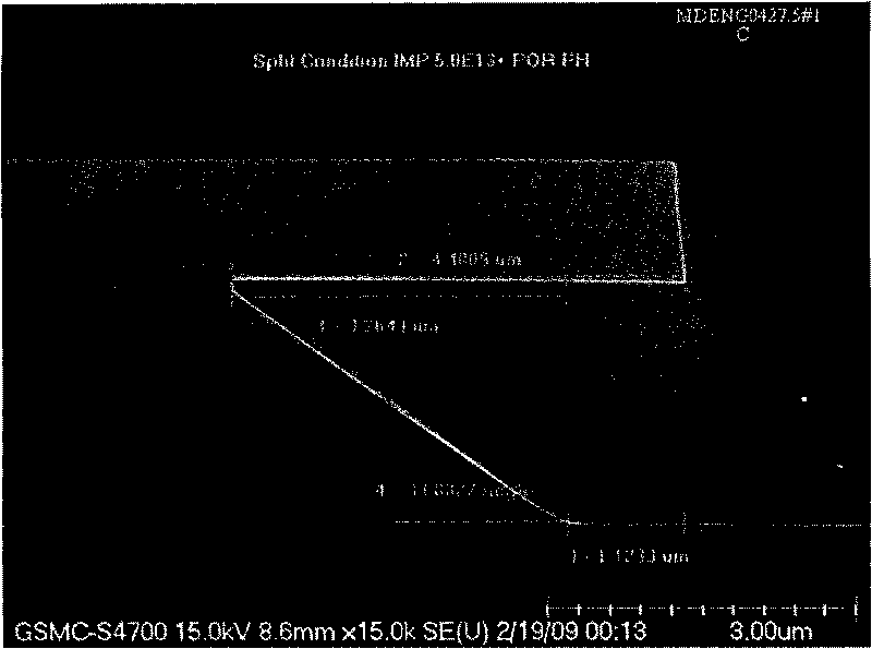
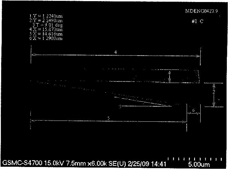
[0023] see figure 2 , which shows the process flow of the oxide layer manufacturing method capable of reducing the slope of the sidewall of the present invention, as shown in the figure, the method of manufacturing the oxide layer capable of reducing the slope of the sidewall of the present invention firstly performs step S20, through the thermal oxidation process in Silicon oxide is grown on the silicon substrate, and the oxidation temperature of the thermal oxidation process is 900 to 1000 degrees Celsius.

[0024] In this embodiment, the oxide layer is a field oxide layer, and its thickness ranges from 2 to 3 microns.

[0025] Then continue to step S21, doping silicon oxide by argon ion implantation process. In this embodiment, the implantation energy of the argon ion implantation process is 80keV, and the dose is...


PUM

PropertyMeasurementUnit
Thicknessaaaaaaaaaa

Abstract

The invention provides a method for manufacturing an oxide layer capable of reducing the gradient of a side wall. In the prior art, silicon oxide is directly subjected to photoetching and wet etching without being washed with hydrofluoric acid buffer corrosive liquid so as to result in larger gradient of the side wall. The method comprises the following steps: firstly, growing the silicon oxide on a silicon substrate through thermal oxidation process; secondly, washing the silicon oxide by using the hydrofluoric acid buffer corrosive liquid, and drying the silicon oxide; thirdly, coating photoresist on the silicon oxide, and baking the photoresist; fourthly, forming a graph of the oxide layer on the photoresist by exposure process; fifthly, developing the graph; sixthly, etching the graph by using the hydrofluoric acid buffer corrosive liquid to form the oxide layer; and finally, removing the photoresist. The method effectively reduces the compactness of the surface of the oxide layer and the adherence force of the oxide layer with the photoresist by washing the silicon oxide with the hydrofluoric acid buffer corrosive liquid before the photoetching and the wet etching processes, thereby effectively reducing the gradient of the side wall, and effectively improving the performance of a device.

Description

technical field [0001] The invention relates to the field of semiconductor manufacturing, in particular to an oxide layer manufacturing method capable of reducing the slope of sidewalls. Background technique [0002] Silicon oxide is one of the most widely used insulating dielectrics in the field of semiconductor manufacturing. It can be used as field oxide layer, gate oxide layer and shallow trench isolation structure (STI), etc. Silicon oxide can be produced by thermal oxidation and chemical vapor deposition. Process production, the thermal oxidation method is suitable for places that require high insulation performance, such as making field oxide layers and gate oxide layers. [0003] In the manufacturing process of semiconductor devices, in order to improve the breakdown characteristics of the devices, some devices need to form a thicker (more than 2 micron) field oxide layer (Field Oxide) on the silicon substrate for isolation. The manufacturing method of the oxide lay...

Claims


Application Information

Patent Timeline
IPC IPC(8): H01L21/3105H01L21/311
Inventor 郭国超
Owner SHANGHAI HUAHONG GRACE SEMICON MFG CORP
Why Eureka
Try Eureka