MEMS wafer level vacuum packaging process
A vacuum packaging, wafer-level technology, used in decorative arts, microstructure devices, manufacturing microstructure devices, etc., can solve the problems of large influence of bonding strength, uneven glass surface, large packaging stress, etc., to achieve airtightness Good, high strength and toughness, simple method
- Summary
- Abstract
- Description
- Claims
- Application Information
AI Technical Summary
Problems solved by technology
Method used
Image
Examples
Embodiment 1
[0027]A MEMS wafer-level vacuum packaging method, comprising the following steps:
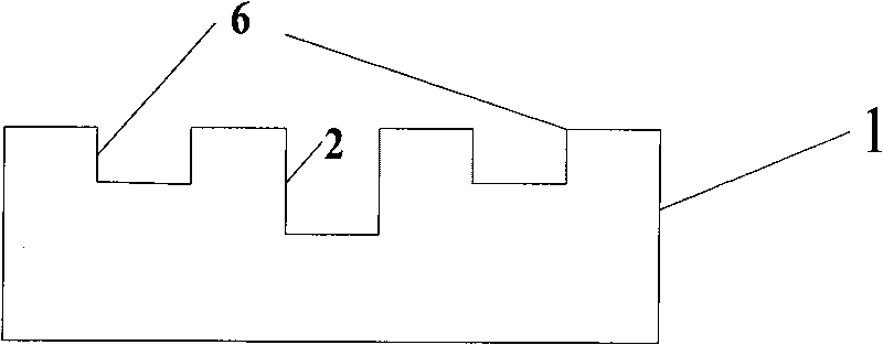
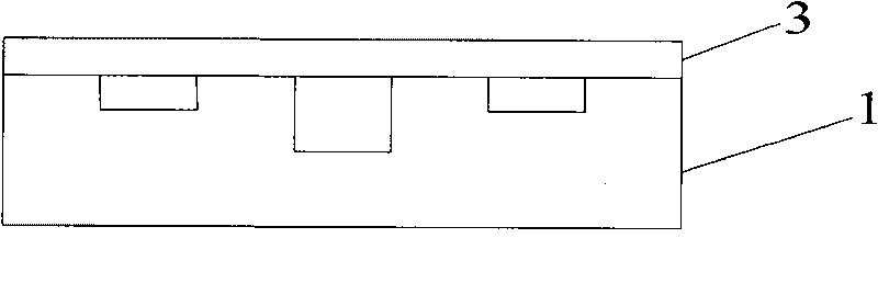
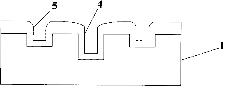
[0028] In the first step, the packaging groove and the annular buffer groove surrounding the packaging groove are etched on the Si wafer (such as a 4-inch wafer) by using Si micromachining technology. First, the packaging groove is etched, and then the buffer groove area is photoetched. The on-chip etched buffer trenches are shallower than the package trenches. When photoetching shallow grooves, the protection of deep packaging grooves can be protected by dry film photoresist, and the micromachining process of the pattern structure on the Si original sheet is a wet etching process or a dry inductively coupled plasma (ICP) etching process. Etching process, reactive ion etching or deep reactive ion etching. The aspect ratio of the packaging groove is determined according to the packaging requirements of the device. It can be less than 1:1 or greater than 1:1. The depth of the ring buffer groove c...
Embodiment 2
[0036] A MEMS wafer-level vacuum packaging method, comprising the following steps:
[0037] In the first step, the packaging groove and the annular buffer groove surrounding the packaging groove are etched on the Si wafer (such as a 4-inch wafer) by using Si micromachining technology. First, the packaging groove is etched, and then the buffer groove area is photoetched. The on-chip etched buffer trenches are shallower than the package trenches. When photoetching shallow grooves, the protection of deep packaging grooves can be protected by dry film photoresist (such as the dry film photoresist series produced by DuPont, USA), and the micromachining process on the Si wafer is dry inductive coupling. Plasma (ICP) etching process, the aspect ratio of the packaging groove is determined according to the packaging requirements of the device, for example, the depth is 300 microns, the width is 400 microns, the depth of the ring buffer groove is smaller than the depth of the packaging ...
PUM
 Abstract
Description
Claims
Application Information


