MEMS wafer level vacuum packaging process

A vacuum packaging, wafer-level technology, applied in decorative arts, microstructure devices, manufacturing microstructure devices, etc., can solve the problems of large influence on bonding strength, uneven glass surface, large packaging stress, etc., and achieve airtightness Good, high strength and toughness, simple method

Active Publication Date: 2011-08-03
SOUTHEAST UNIV
View PDF0 Cites 0 Cited by
  • Summary
  • Abstract
  • Description
  • Claims
  • Application Information

AI Technical Summary

Problems solved by technology

The reason is that as the depth of the molded cavity increases, more glass needs to be supplemented into the silicon cavity of the mold around the microcavity, so that the thickness of the glass around the microcavity of the glass wafer decreases, so that it is different from the plane of the non-flowing part of the glass wafer. Causes a large height difference, resulting in uneven glass surface
The surface roughness has a great influence on the bonding strength of anodic bonding, and also leads to a large package stress caused by the bonding process

Method used


Image

  • MEMS wafer level vacuum packaging process
  • MEMS wafer level vacuum packaging process
  • MEMS wafer level vacuum packaging process

Examples


Embodiment 1

[0027]A MEMS wafer-level vacuum packaging method, comprising the following steps:

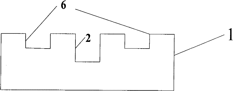
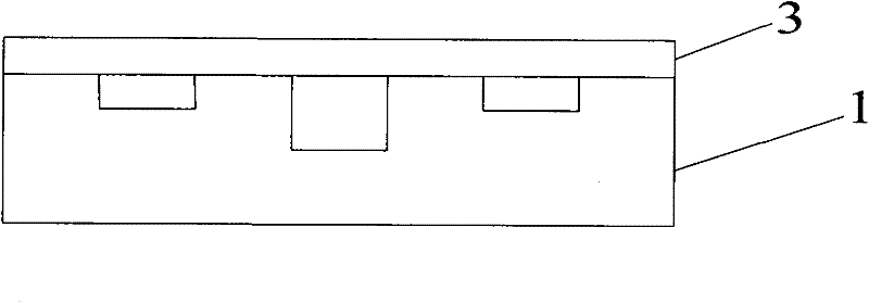
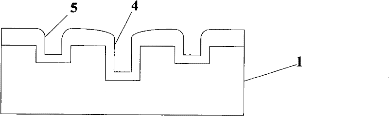
[0028] In the first step, the packaging groove and the annular buffer groove surrounding the packaging groove are etched on the Si wafer (such as a 4-inch wafer) by using Si micromachining technology. First, the packaging groove is etched, and then the buffer groove area is photoetched. The on-chip etched buffer trenches are shallower than the package trenches. When photoetching shallow grooves, the protection of deep packaging grooves can be protected by dry film photoresist, and the micromachining process of the pattern structure on the Si original sheet is a wet etching process or a dry inductively coupled plasma (ICP) etching process. Etching process, reactive ion etching or deep reactive ion etching. The aspect ratio of the packaging groove is determined according to the packaging requirements of the device. It can be less than 1:1 or greater than 1:1. The depth of the ring buffer groove c...

Embodiment 2

[0036] A MEMS wafer-level vacuum packaging method, comprising the following steps:

[0037] In the first step, the packaging groove and the annular buffer groove surrounding the packaging groove are etched on the Si wafer (such as a 4-inch wafer) by using Si micromachining technology. First, the packaging groove is etched, and then the buffer groove area is photoetched. The on-chip etched buffer trenches are shallower than the package trenches. When photoetching shallow grooves, the protection of deep packaging grooves can be protected by dry film photoresist (such as the dry film photoresist series produced by DuPont, USA), and the micromachining process on the Si wafer is dry inductive coupling. Plasma (ICP) etching process, the aspect ratio of the packaging groove is determined according to the packaging requirements of the device, for example, the depth is 300 microns, the width is 400 microns, the depth of the ring buffer groove is smaller than the depth of the packaging ...


PUM

PropertyMeasurementUnit
depthaaaaaaaaaa
widthaaaaaaaaaa

Abstract

The invention discloses an MEMS glass microcavity vacuum packaging process with long vacuum maintaining time, which comprises the following steps of: firstly, etching a deep packaging groove on a Si wafer by using an Si microprocessing process and etching a relatively shallower annular vacuum buffer groove at the periphery of the deep packaging groove; then bonding the Si wafer etched with the microgroove and a glass wafer so that the glass wafer and the specific pattern form a packaging cavity; heating and preserving the temperature of the bonded wafer at atmosphere pressure and leading softened glass to flow into the packaging cavity by a pressure difference inside and outside the cavity so as to form a microcavity structure corresponding to the microcavity pattern structure; cooling and annealing and removing stress of the wafer at normal pressure; then corroding to remove the Si wafer; and carry out anode bonding on the Si wafer and the glass wafer at the atmosphere of 1Pa-10Pa toform the integral vacuum packaging. The invention improves the maintaining capability of vacuum degree in the packaging cavity by manufacturing the annular vacuum buffer cavity at the periphery of the packaging cavity.

Description

technical field [0001] The invention relates to a MEMS (micro-electro-mechanical system) packaging technology, in particular to a MEMS wafer-level vacuum packaging method. Background technique [0002] In the field of MEMS packaging, since devices generally contain movable parts, it is necessary to use a micron-sized microcavity structure to hermetically package the device during packaging, so that the movable parts have room for movement and provide physical protection for the device. Some such as Devices such as resonators, gyroscopes, and accelerometers also require a vacuum and airtight packaging environment. The cavity made of inorganic material glass can provide a better vacuum and sealing environment, and the anodic bonding process can provide very good air tightness, which is the most commonly used vacuum sealing bonding process. The vacuum packaging of MEMS devices can be achieved by forming a microcavity structure on Pyrex7740 glass and anodic bonding with a Si su...

Claims


Application Information

Patent Timeline
Patent Type & Authority Patents(China)
IPC IPC(8): B81C1/00
Inventor 尚金堂陈波寅张迪徐超柳俊文唐洁影黄庆安
Owner SOUTHEAST UNIV
Why Eureka
Try Eureka