Package structure and manufacture method thereof

A packaging structure and patterning technology, applied in semiconductor/solid-state device manufacturing, electrical components, electrical solid-state devices, etc., can solve problems such as device failure, achieve the effect of improving packaging reliability and avoiding collapse

Inactive Publication Date: 2010-06-09
SEMICON MFG INT (SHANGHAI) CORP
View PDF0 Cites 32 Cited by
  • Summary
  • Abstract
  • Description
  • Claims
  • Application Information

AI Technical Summary

Problems solved by technology

Since the stress buffer layer 40 covers the passivation layer 30, the stress buffer layer 40 is relatively flat, and there is often stress concentration in the edge region between the pillar 60 and the stress buffer layer 40, because there is no mechanical gap between the underfill 91 and the stress buffer layer 40 Lock (Mechanical Lock), the stress concentration result is easy to form cracks at the interface between the underfill glue 91 and the stress buffer layer 40 and expand rapidly, eventually leading to device failure

Method used


Image

  • Package structure and manufacture method thereof
  • Package structure and manufacture method thereof
  • Package structure and manufacture method thereof

Examples


Embodiment Construction

[0046] In order to make the object, technical solution and advantages of the present invention clearer, the present invention will be further described in detail below in conjunction with the accompanying drawings.

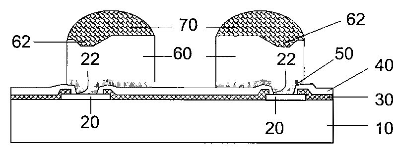
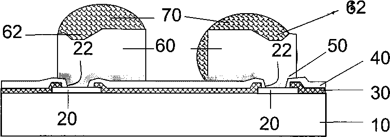
[0047] Image 6 Shown is a structural schematic diagram of an embodiment of the packaging structure of the present invention. Such as Image 6 As shown, the package structure includes a semiconductor substrate 10 , a contact pad 20 , a passivation layer 30 , a stress buffer layer 40 , and a stud bump composed of an UBM seed layer 50 , pillars 60 , and solder bumps 70 . 10 is a semiconductor substrate of a chip, and at least one active device is formed in the semiconductor substrate 10 . More than one contact pad (I / O port) 20 is formed on the semiconductor substrate 10 and is usually made of aluminum, copper, or an alloy material of the aforementioned metals. The passivation layer 30 is covered on the semiconductor substrate 10, and the contact pad 20 is expose...


PUM


Abstract

The invention provides a package structure and a manufacture method thereof, belonging to the technical field of micro-electronics manufacture. The package structure comprises a semiconductor substrate, a contact welding pad, a passivation layer, a stress buffer layer and columnar lugs formed on the buffer layer, wherein the areas corresponding to any of the columnar lug structures in the stress buffer layer are provided with main openings and one or more than one auxiliary opening, the main openings and the auxiliary openings are distributed evenly in the composition plane range of the corresponding columnar lugs. The package structure provided in the invention can avoid welding flux from collapsing during reflux in the forming process of columnar lugs and has the characteristic of high reliability.

Description

technical field [0001] The invention belongs to the technical field of semiconductor manufacturing, in particular to the packaging technology of electrical and mechanical connections of chips, and in particular to a packaging structure of stud bumps and a manufacturing method thereof. Background technique [0002] As the interconnection density of the chip and the number of chip pins (Pin) increase, the distance between the external connection ports (I / O ports) on the chip is getting smaller and smaller, and the operating speed of the circuit is getting higher and higher. The advanced gold wire packaging technology can no longer meet the requirements of high-performance circuits due to the large delay of circuit signals. The emergence of solder bump (Solder Bump) technology shortens the connection distance between the chip and the next level of packaging, reducing the signal delay caused by the chip package; at the same time, the I / O ports on the chip can be arranged on the ...

Claims


Application Information

Patent Timeline
Patent Type & Authority Applications(China)
IPC IPC(8): H01L23/485H01L21/60
CPCH01L2224/92125H01L2224/73204H01L24/11H01L2224/16225H01L2224/32225H01L2224/11H01L2924/00H01L2924/00012
Inventor 朱奇农李德君
Owner SEMICON MFG INT (SHANGHAI) CORP
Why Eureka
Try Eureka