GaN based LED epitaxial wafer of graphical substrate and method for preparing same

A technology for LED epitaxial wafers and graphic substrates, which is applied in the manufacture of semiconductor/solid-state devices, electrical components, circuits, etc., can solve the problems of not improving the quality of GaN crystals, poor quality of GaN epitaxial crystals, and singleness, and improve the external quantum efficiency. , The effect of improving crystal quality and improving light output efficiency

Inactive Publication Date: 2010-06-16
SHENZHEN CENTURY EPITECH LEDS
View PDF0 Cites 37 Cited by
  • Summary
  • Abstract
  • Description
  • Claims
  • Application Information

AI Technical Summary

Problems solved by technology

[0008] The above-mentioned existing methods only improve a certain performance of the LED, or improve the quality of GaN crystal, or improve the light extraction efficiency of GaN-based LED, and cannot improve the poor quality of GaN epitaxial crystal and GaN luminescence at the same time. The problem of low light extraction efficiency of the device

Method used


Image

  • GaN based LED epitaxial wafer of graphical substrate and method for preparing same
  • GaN based LED epitaxial wafer of graphical substrate and method for preparing same
  • GaN based LED epitaxial wafer of graphical substrate and method for preparing same

Examples


Embodiment 1

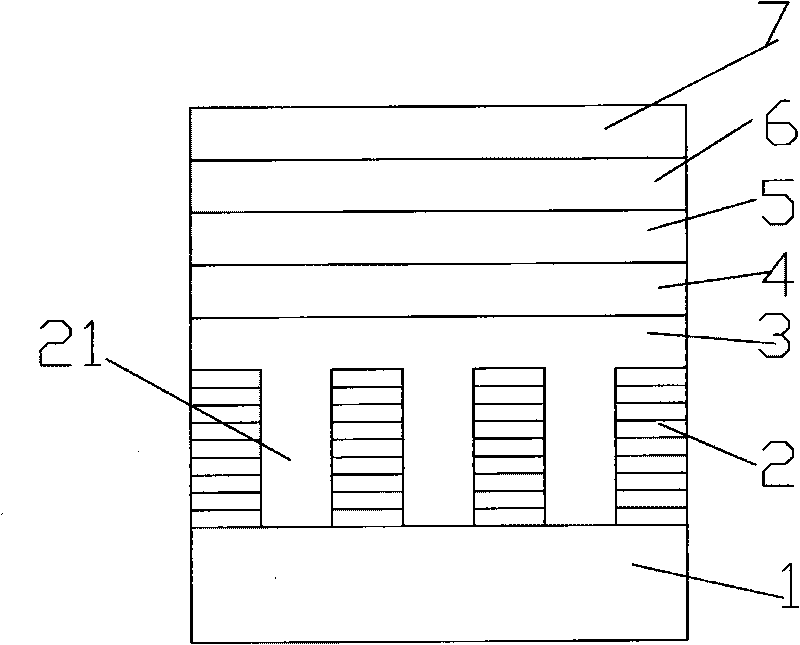
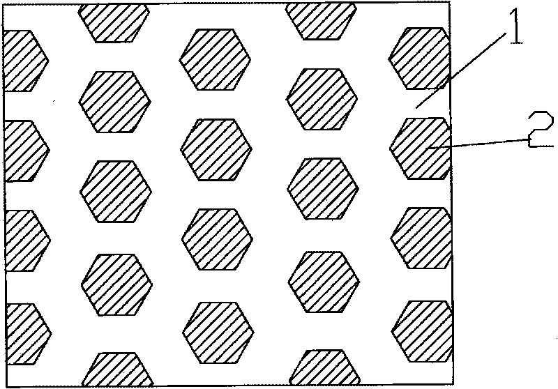
[0046] like figure 2 As shown, the pattern structure described in the embodiment of the present invention is a regular hexagon, the width a of the pattern structure is 6 micrometers, and the distance b between adjacent patterns is 4 micrometers; the SiO 2 The number of alternating cycles with SiON is 8 times; the SiO described in the embodiment of the present invention 2 Alternating layers with SiON each have a thickness of 58nm and 64nm, respectively.

Embodiment 2

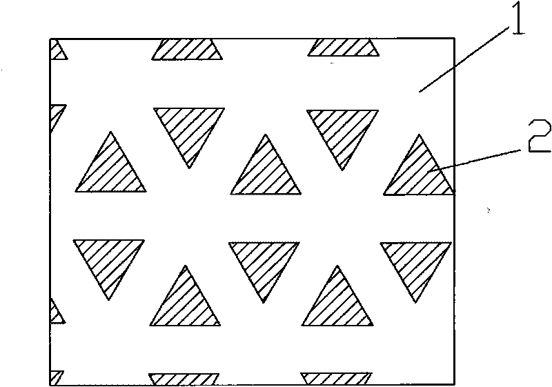
[0048] like image 3 As shown, the pattern structure described in the embodiment of the present invention is an equilateral triangle, the width a of the pattern structure is 3 microns, and the spacing b between adjacent patterns is 2 microns; the SiO 2 The number of alternating cycles with SiON is 16 times; the SiO described in the embodiment of the present invention 2 Alternating layers with SiON each have a thickness of 68nm and 75nm, respectively.

Embodiment 3

[0050] like Figure 4 As shown, the pattern structure described in the embodiment of the present invention is a square, the width a of the pattern structure is 10 microns, and the distance b between adjacent patterns is 6 microns; the SiO 2 The number of alternating cycles with SiON is 4 times; the SiO described in the embodiment of the present invention 2 Alternating layers with SiON each have a thickness of 58nm and 64nm, respectively.


PUM


Abstract

The invention provides a GaN based LED epitaxial wafer of a graphical substrate and a method for preparing the same. In the GaN based LED epitaxial wafer of the graphical substrate, the substrate of the epitaxial wafer comprises a distributed DBR reflecting layer which has a layering structure formed by periodical alternative growth of two transparent materials with different refractive indexes, and the DBR reflecting layer having the layering structure forms at least two graphical structures, which are spaced, on the substrate; a window area is formed between the graphical structures, and the GaN epitaxial layer can be epitaxially grown from the window area; because the growing direction of the crystals is vertical to the original motion direction of dislocations, and a mask layer blocks the majority of motion of the extended dislocations, so that the epitaxial growth of the invention can greatly reduce the density of the extended dislocations in the epitaxial layer, and improve the crystal quality of the GaN epitaxial film; and simultaneously, because the DBR reflecting layer structure on the graphical substrate is the layering structure formed by the periodical alternative growth of two materials with different refractive indexes, the light transmitted downward by an active area can be reflected to the upper surface of the output light and the light outputting efficiency of the LEDs is greatly improved.

Description

technical field [0001] The invention relates to the field of compound semiconductor epitaxial wafers, in particular to an epitaxial wafer with a patterned substrate GaN-based LED. [0002] The invention also relates to a method for preparing an epitaxial wafer with a patterned substrate GaN-based LED. Background technique [0003] Light-emitting diode (LED) is a kind of solid-state light-emitting device that can directly convert electrical energy into visible light and radiant energy. It has the advantages of long working life, high luminous efficiency, no pollution, light weight, and small size. Widely used in indoor and outdoor large-screen display, backlight display, lighting, decoration, traffic lights and other fields. The GaN material system is the most mature material for preparing blue, green, purple and ultraviolet LEDs. The research on GaN materials began in the 1930s. In 1991, someone in the industry discovered that the method of using a low-temperature growth G...

Claims


Application Information

Patent Timeline
Patent Type & Authority Applications(China)
IPC IPC(8): H01L33/00
CPCH01L21/0242H01L33/44H01L33/12H01L33/14H01L21/0262H01L21/0254H01L21/02639H01L33/0075H01L21/02647
Inventor 胡加辉朱国雄吴煊梁廖家明沈志强
Owner SHENZHEN CENTURY EPITECH LEDS
Why Eureka
Try Eureka