
Method for preparing microwave power device by composite mask plate

A microwave power and reticle technology, which is applied in semiconductor/solid-state device manufacturing, electrical components, circuits, etc., can solve the problems of microwave performance deterioration of microwave power devices, unequal distance between the emission area and the base ohmic contact area, etc., to achieve Improves microwave performance and eliminates the effect of unequal spacing

Active Publication Date: 2011-06-29
THE 13TH RES INST OF CHINA ELECTRONICS TECH GRP CORP
View PDF0 Cites 0 Cited by
  • Summary
  • Abstract
  • Description
  • Claims
  • Application Information

AI Technical Summary

Problems solved by technology

[0003] The technical problem to be solved by the present invention is that the registration deviation caused by two photolithography when preparing the emitter region and the base ohmic contact region in the traditional process makes the spacing between the emitter region and the base ohmic contact region not equidistant, so that Problems of Microwave Performance Deterioration of Microwave Power Devices

Method used


Image

  • Method for preparing microwave power device by composite mask plate
  • Method for preparing microwave power device by composite mask plate
  • Method for preparing microwave power device by composite mask plate

Examples


Embodiment Construction

[0022] The present invention will be described in further detail below in conjunction with the accompanying drawings.

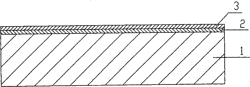
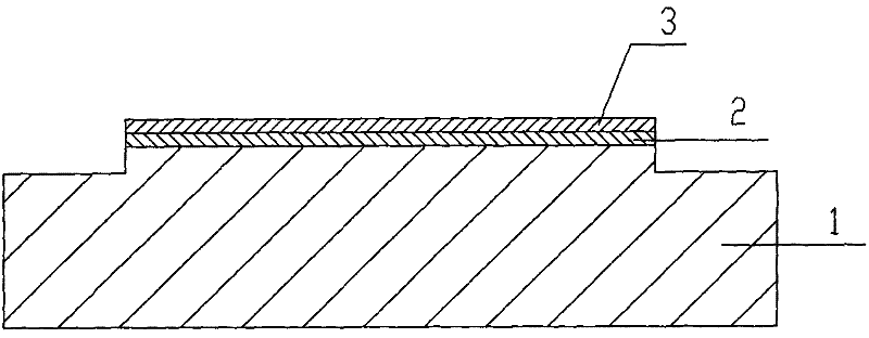
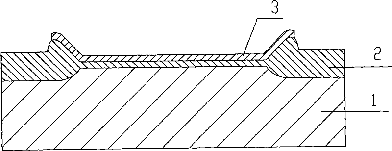
[0023] A method for preparing a microwave power device using a composite mask provided by the present invention includes: depositing a protective layer of silicon oxide 2 and silicon nitride 3 on a silicon wafer 1, and forming an emission region 10 and base ohmic contact region 13, and then deposit metal layer to prepare metal lead-out electrodes to form emitter 14 and base 15; in this method, composite mask plate 6 is used to complete photolithography at one time, and etch to form emission region window and base Very ohmic contact region window; selectively cover the base ohmic contact region window or emission region window by coating photoresist 7, continue etching and ion implantation to form emission region 10 or Base ohmic contact region 13; cover the emitter region 10 or base ohmic contact region 13 formed after the above-mentioned ion implantation wit...


PUM


Abstract

The invention discloses a method for preparing a microwave power device by a composite mask plate. The method adopts a selective oxidation technology and a surface planarization technology to realize a locating field region and an active region of a chip in the same focal plane and to realize an isoplanar structure. The invention adopts the same composite mask plate for photo-etching and etching to form an emitting region and a doping window of a base electrode ohm contact region, and then the doping of the emitting region and the base electrode ohm contact region is achieved. Furthermore, self-alignment of the emitting region and the base electrode ohm contact region of a bipolar device chip is realized in combination with a sidewall protection technology. The method realizes a photo-etching technology of sub-micron and deep sub-micron graphics, and equalizes spacing between the emitting region and the base electrode ohm contact region through one photo-etching technology, thereby achieving the purpose of improving microwave properties of the microwave power device.

Description

technical field [0001] The invention relates to a method for preparing a power device, in particular to a method for preparing a microwave power device by using a composite mask plate. Background technique [0002] In recent years, the operating frequency of silicon microwave power devices has reached the S-band, and the output power has reached hundreds of watts, which is close to the frequency limit of silicon-based microwave power devices. In the design of such device chips, hundreds of high-density, high-resolution chips are required. The operating frequency and high output power of the device can be realized by sub-micron scale pattern processing with high aspect ratio, which poses a challenge to the traditional silicon microwave power device process. First of all, the traditional silicon planar processing technology will cause the chip field region and the active region to not be on the same plane, and the chip field region will be 0.6 μm to 1.0 μm higher than the base...

Claims


Application Information

Patent Timeline
Patent Type & Authority Patents(China)
IPC IPC(8): H01L21/331
Inventor 邓建国刘英坤胡顺欣
Owner THE 13TH RES INST OF CHINA ELECTRONICS TECH GRP CORP
Learn More