

Perfusion method and device of protection glue for chip insulation
A protective glue and chip technology, applied in electrical components, semiconductor/solid-state device manufacturing, circuits, etc., can solve the problems affecting the long-term stability of protective glue, not taken into account, etc., to improve surface breakdown voltage, good insulation effect, simple structure
- Summary
- Abstract
- Description
- Claims
- Application Information
AI Technical Summary
Problems solved by technology
Method used
Image

Examples
Embodiment Construction
[0032] The present invention will be described in detail below with reference to the drawings and specific embodiments.
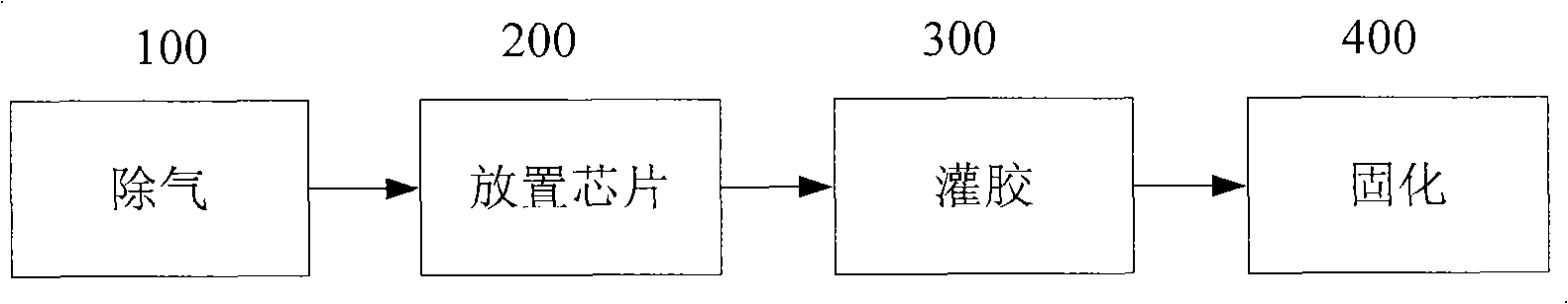
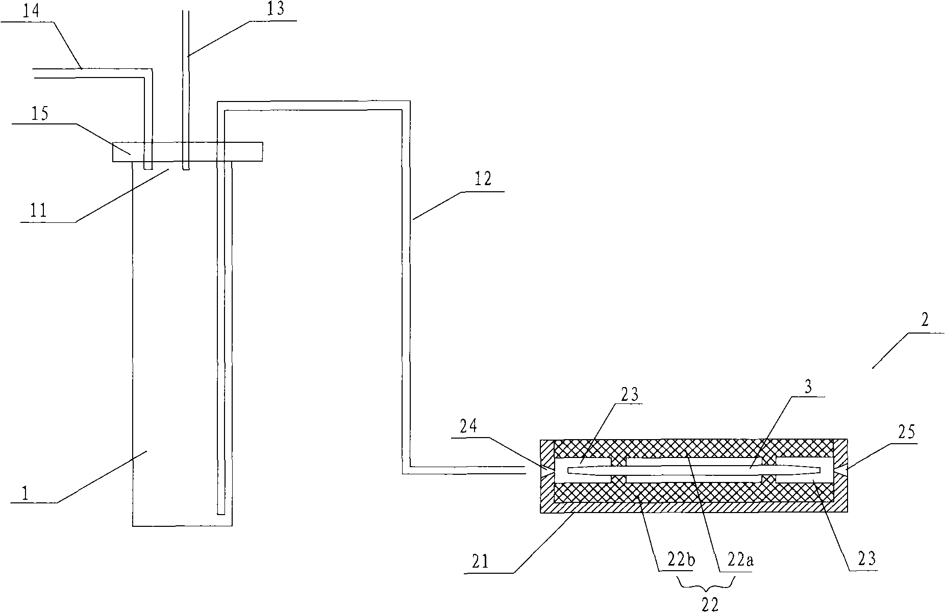
[0033] figure 2 It is a schematic flow chart of the protective glue pouring method of the present invention. image 3 It is a schematic diagram of the structure of the protective glue pouring device of the present invention.
[0034] Such as figure 2 As shown, the protective glue pouring method for chip insulation of the present invention includes: a degassing step 100, a chip placement step 200, a glue filling step 300, and a curing step 400.
[0035] In the degassing step 100, first pour the protective glue into figure 2 After the airtight container 1 is shown, the airtight container is evacuated and kept under vacuum for a period of time, so that the air bubbles in the protective glue are discharged due to the negative pressure of the airtight container.
[0036] The protective rubber added is preferably silicone rubber, such as dimethyl silicone rubber, meth...
PUM
 Abstract
Description
Claims
Application Information