

Optical film and manufacturing method therefor, anti-glare film, polarizing element with optical layer, and display device
A technology of optical layer and optical film, which is applied in the field of optical film, can solve the problems that are difficult to realize at the same time, and the anti-glare property is reduced.
- Summary
- Abstract
- Description
- Claims
- Application Information
AI Technical Summary
Problems solved by technology
Method used
Image

Examples
no. 1 approach
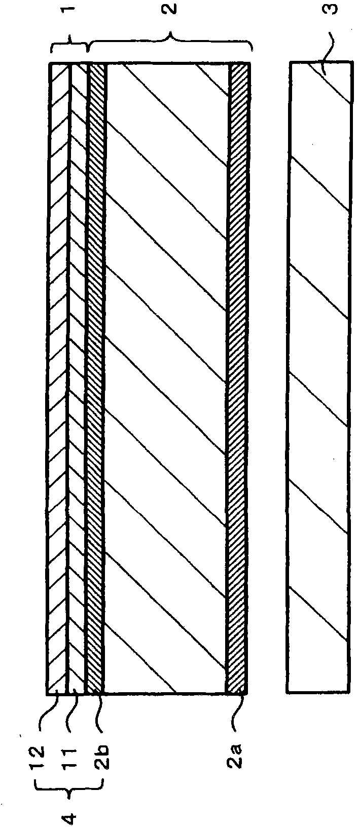
[0105] (1-1) Structure of liquid crystal display device
[0106] image 3 One example of the structure of the liquid crystal display device according to the first embodiment of the present invention is shown. Such as image 3 As shown, the liquid crystal display device includes a backlight 3 that emits light, and a liquid crystal panel 2 that modulates the light emitted by the backlight 3 in time and space to display images. Polarizers 2a and 2b are provided on both surfaces of the liquid crystal display panel 2, respectively. The anti-glare film 1 is provided on a polarizer 2b provided on the display surface side of the liquid crystal display panel 2 . In the present invention, the polarizer 2 b having the antiglare film 1 or the antiglare layer on one main surface is referred to as an antiglare polarizer 4 .
[0107] For example, a direct type backlight, an edge type backlight, or a flat light source type backlight can be used as the backlight 3 . The backlight 3 includ...
no. 2 approach
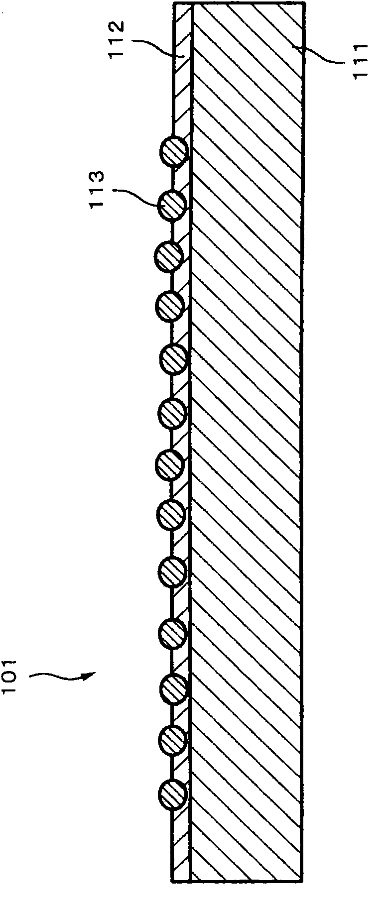
[0177] (2-1) Structure of anti-glare film
[0178] Figure 7 One example of the structure of the antiglare film according to the second embodiment of the present invention is shown. Such as Figure 7 As shown, the difference between the anti-glare film 1 of the second embodiment and the first embodiment is that a low-refractive-index layer 14 is further provided on the anti-glare film 12 . Since the base material 11 and the antiglare layer 12 are the same as those in the first embodiment, they are assigned the same reference numerals and their descriptions are omitted.
[0179] Such as Figure 7 As shown, the low refractive index layer 14 is preferably arranged to follow the undulations on the surface of the antiglare layer. More preferably, the low refractive index layer 14 has substantially the same thickness, and the undulations of the surface of the antireflection layer have substantially the same gentle undulations as the undulations of the surface of the antiglare la...
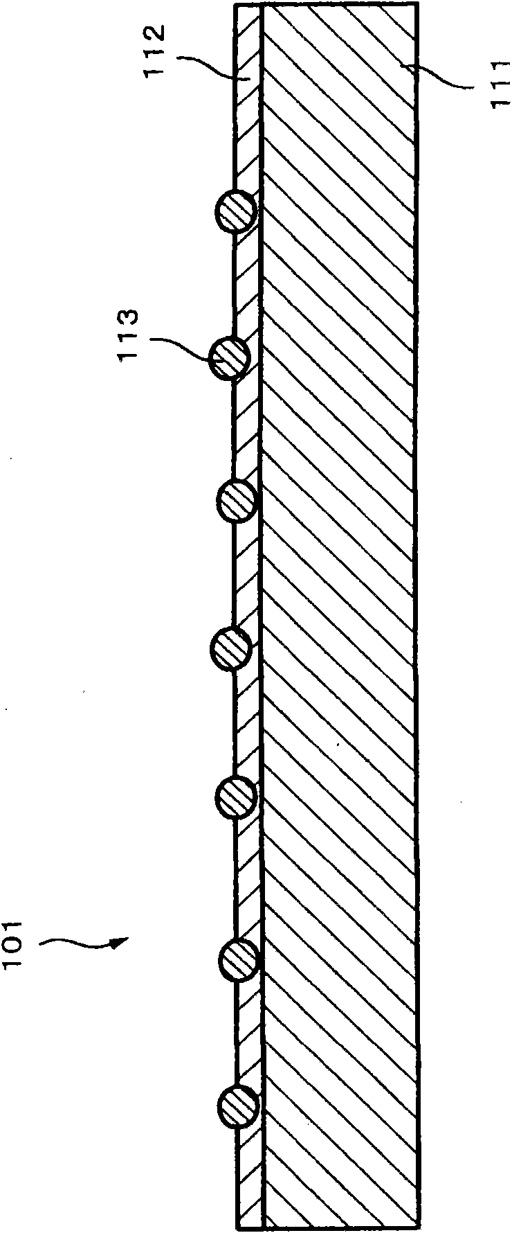
no. 3 approach
[0197] Figure 9 One example of the structure of the antiglare film according to the third embodiment of the present invention is shown. Such as Figure 9 As shown, the difference between the anti-glare film 1 and the above-mentioned first embodiment is that a multi-layer anti-reflection layer is provided on the anti-glare layer 12 . Since the base material 11 and the antiglare layer 12 are the same as those in the first embodiment described above, they are assigned the same reference numerals and their descriptions are omitted.
[0198] The multilayer antireflection layer 16 is a laminated film including a low refractive index layer 16L and a high refractive index layer 16H. Preferably, the lamination number of the low-refractive index layer 16L and the lamination number of the high-refractive index layer 16H are appropriately selected according to required characteristics. Examples of materials that can be used for the low refractive index layer 16L include, but are not p...
PUM
| Property | Measurement | Unit |
|---|---|---|
| particle size | aaaaa | aaaaa |
| thickness | aaaaa | aaaaa |
| particle size | aaaaa | aaaaa |
Abstract
Description
Claims
Application Information