Preparation method of Cu2ZnSnS4 semiconductor material

A technology of semiconductor and ammonium sulfide, which is applied in the field of preparation of Cu2ZnSnS4 semiconductor materials, can solve the problems of vacuum or gas protection in the preparation process, complex vulcanization process, difficult control of product stoichiometry, etc., to achieve easy control and adjustment, simple preparation process, low cost effect

Inactive Publication Date: 2010-07-21
HEFEI UNIV OF TECH
View PDF4 Cites 17 Cited by
  • Summary
  • Abstract
  • Description
  • Claims
  • Application Information

AI Technical Summary

Problems solved by technology

Cu 2 ZnSnS 4 Thin films and corresponding n-CdS/p-Cu 2 ZnSnS 4 Thin-film solar cells have a photoelectric conversion efficiency of 6.9%; Hironori Katagiri et al. (Thin Solid Films, 2007, 515: 5997-5999) prepared Cu 2 ZnSnS 4 Thin-film and thin-film solar cells have achieved a photoelectric conversion efficiency of 5.74%; Russian patent RU2347299C1 prepared Cu 2 ZnS

Method used


Image

  • Preparation method of Cu2ZnSnS4 semiconductor material
  • Preparation method of Cu2ZnSnS4 semiconductor material

Examples


Embodiment 1

[0015] (1), 8.00g ammonium sulfide solution (sulfur content 8%) and 92.0g distilled water are mixed uniformly, suction filtration, obtain filtrate (A);

[0016] (2) Dissolve 1.12g of stannous chloride in 8.00ml of concentrated hydrochloric acid, dilute with 100.0g of distilled water, then add 0.54g of zinc chloride and 1.87g of copper chloride, stir evenly, and filter with suction. Add the filtrate (A) dropwise while magnetically stirring. After the dropwise addition, continue stirring for 30 min, filter with suction, and wash twice with 100 mL of distilled water to obtain a filter cake;

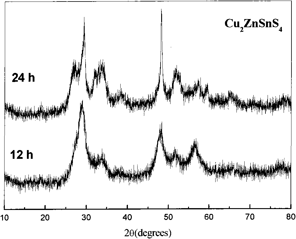
[0017] (3) The filter cake was mixed with 25.0 g of distilled water, then transferred to an autoclave, and kept at 220° C. for 72 hours. After cooling to room temperature, the resulting mixture was rotary evaporated (85 °C, 0.09 MPa) to remove distilled water to obtain a crude product, which was dried in vacuum at 70 °C for 6 h to obtain Cu 2 ZnSnS 4 semiconductors.

Embodiment 2

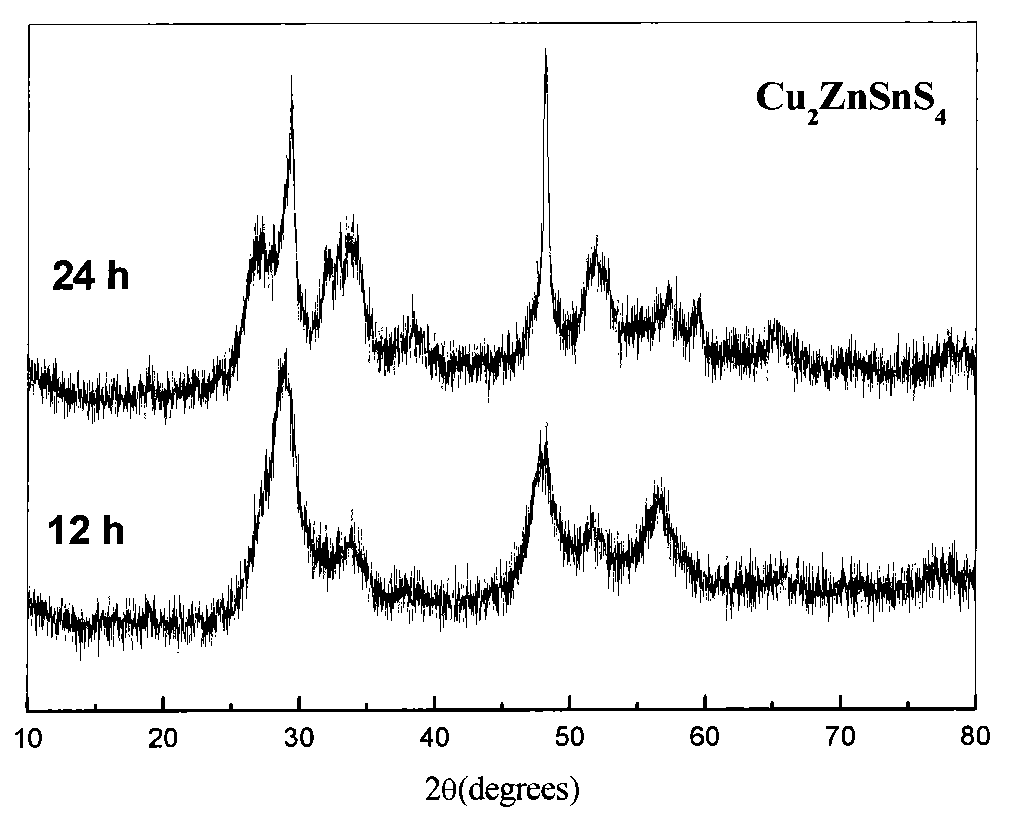
[0019] Dissolve 1.12g of stannous chloride in 8.00ml of concentrated hydrochloric acid, dilute with 100.0g of distilled water, then add 0.82g of zinc chloride and 1.87g of copper chloride, stir evenly, filter with suction, and drop the filtrate (B) while stirring magnetically Add the filtrate (A), after the dropwise addition, continue to stir for 30 min, filter with suction, and wash twice with 100 mL of distilled water to obtain a filter cake; others are the same as in Example 1.

Embodiment 3

[0021] Dissolve 1.12g of stannous chloride in 8.00ml of concentrated hydrochloric acid, dilute with 100.0g of distilled water, then add 0.68g of zinc chloride and 1.87g of copper chloride, stir evenly, filter with suction, and drop the filtrate (B) while stirring magnetically Add the filtrate (A), after the dropwise addition, continue to stir for 30 min, filter with suction, and wash twice with 100 mL of distilled water to obtain a filter cake; others are the same as in Example 1.


PUM


Abstract

The invention discloses a preparation method of Cu2ZnSnS4 semiconductor material and the method uses a mixed solution of stannous chloride, zinc chloride and copper chloride and ammonium sulfide solution as raw materials. The method comprises the following steps: firstly performing solution co-precipitation by using the raw materials according to a ratio, secondly performing high pressure hydrothermal treatment, and separating to obtain the Cu2ZnSnS4 semiconductor material. The methods of solution co-precipitation and high pressure hydrothermal treatment are adopted to prepare the Cu2ZnSnS4 semiconductor material and the method has the advantages that the stoichiometric ratio of the product is easy to control and can be adjusted, the preparation technology is simple, the cost is low, the method is environmentally friendly, etc. the obtained material can be used as absorbing layer to be used in thin film solar cells.

Description

technical field [0001] The invention relates to a preparation method for thin film solar cell semiconductor materials, specifically a Cu 2 ZnSnS 4 Methods for the preparation of semiconductor materials. Background technique [0002] Cu 2 ZnSnS 4 It does not contain low-abundance elements such as Ga, In, Se, and toxic elements such as Cd. It is a low-cost, environmentally friendly semiconductor material, and its band gap is about 1.5eV, which matches the solar spectrum and has a high absorption coefficient. 10 4 cm -1 , meeting the requirements of compound thin film solar cells, is a very important thin film solar cell absorber material. [0003] At present, the preparation of Cu at home and abroad 2 ZnSnS 4 Semiconductor thin films mainly include methods such as vapor deposition of metal precursors followed by vulcanization and magnetron sputtering. Cu 2 ZnSnS 4 Thin films and corresponding n-CdS / p-Cu 2 ZnSnS 4 Thin-film solar cells have a photoelectric conversi...

Claims


Application Information

Patent Timeline
IPC IPC(8): C01G19/00
CPCY02P70/50
Inventor 史成武刘清安桃李史高杨陈柱
Owner HEFEI UNIV OF TECH
Why Eureka
Try Eureka