

Encoding and decoding method for crosstalk resistant on-chip bus and encoding and decoding device thereof
A bus encoding and bus technology, which is applied in the field of microelectronics, can solve the problems of unencoded method power consumption optimization, increased chip area redundancy, and large encoding circuit delay, etc., to eliminate worst-case crosstalk, reduce time overhead, and reduce inserted effect
- Summary
- Abstract
- Description
- Claims
- Application Information
AI Technical Summary
Problems solved by technology
Method used
Image

Examples
Embodiment Construction
[0049] In order to make the objects, features and advantages of the present invention more comprehensible, preferred embodiments of the present invention will be described in detail below together with the accompanying drawings.
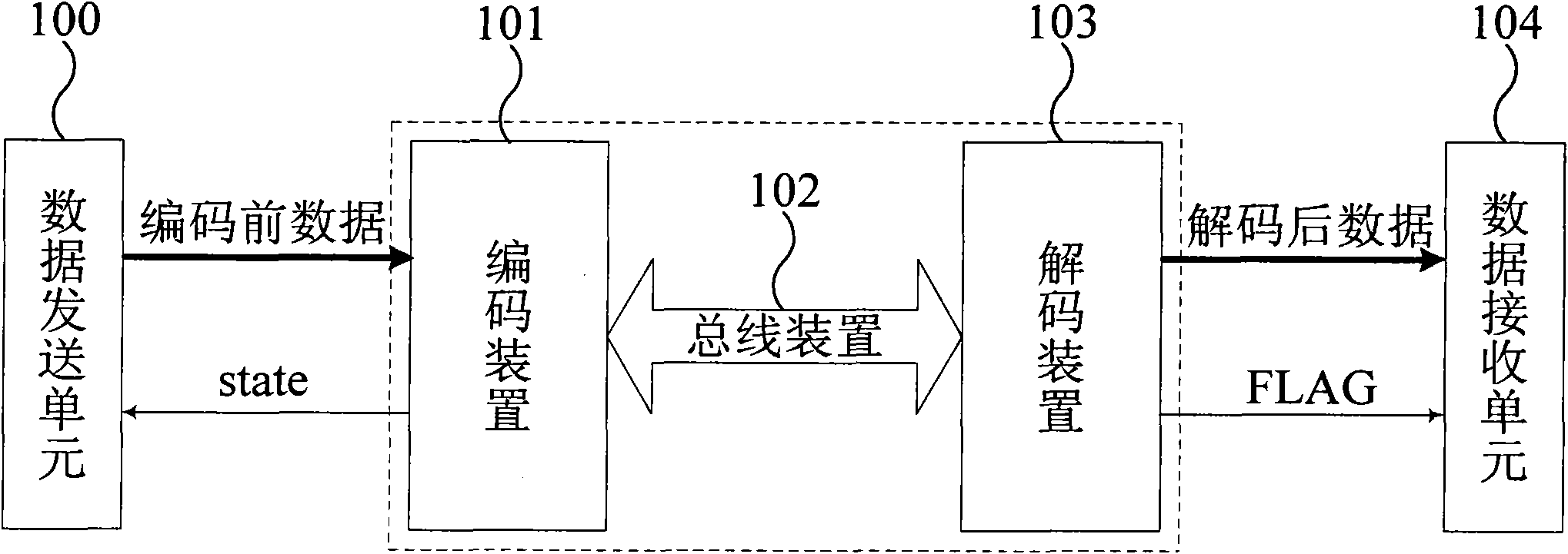
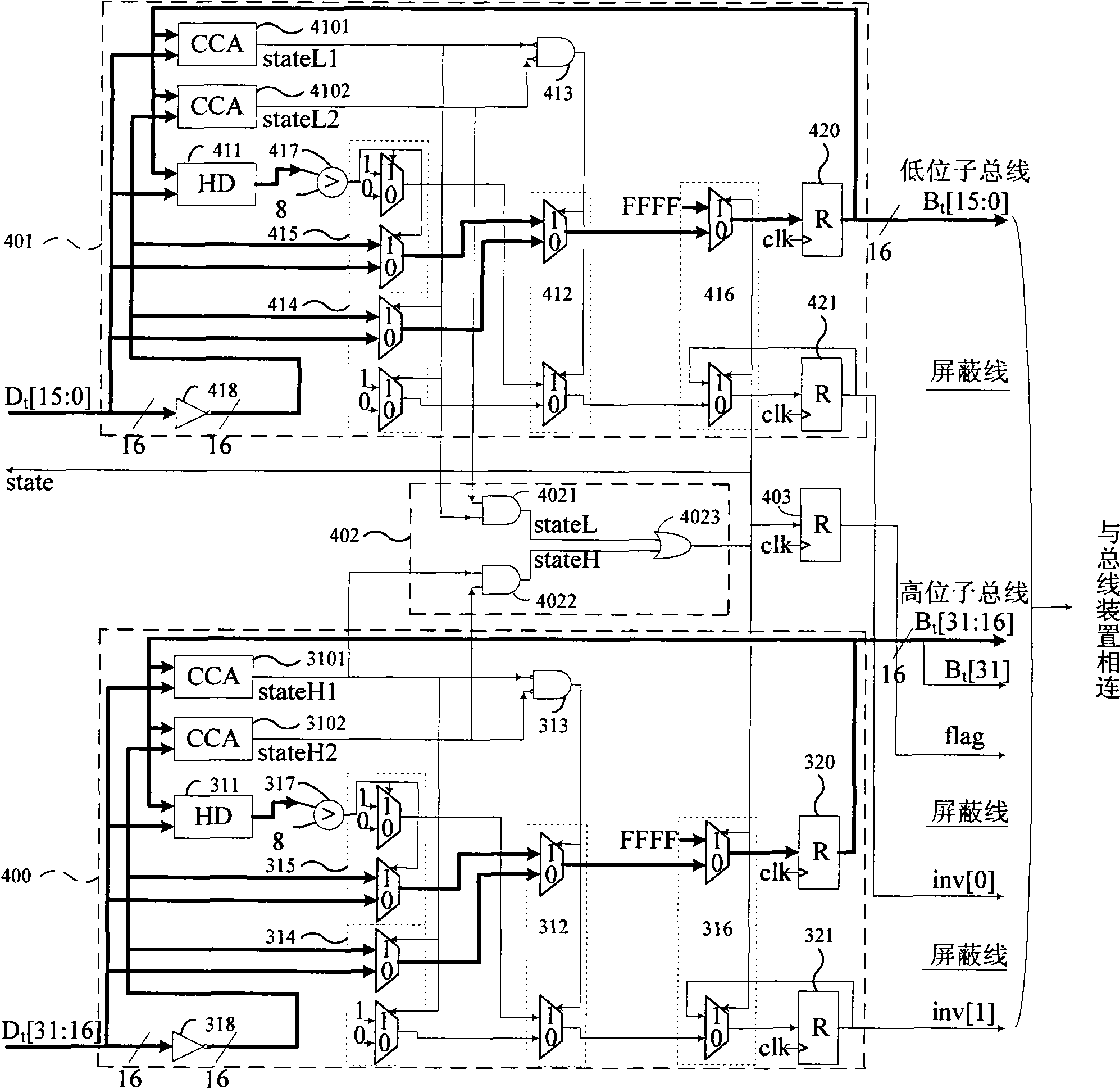
[0050] refer to figure 1 , the anti-crosstalk on-chip bus codec device of the present invention includes:
[0051] A data sending unit 100 , an encoding device 101 , a bus device 102 , a decoding device 103 and a data receiving unit 104 . Wherein, the output terminal of the data transmission unit 100 is connected with the input terminal of the encoding device 101, and transmits the original data to the encoding device 101 according to the state signal state output by the encoding device 101; Converted into coded data words, and then transmitted to the bus device 102; the bus device 102 connects the output of the encoding device 101 and the input of the decoding device 103, and the coded data word is transmitted to the decoding device 103 via the bus...
PUM
 Abstract
Description
Claims
Application Information