
Manufacturing method of ceramic electronic component

A technology of ceramic electronic components and production methods, which is applied in the direction of electrical components, inductance/transformer/magnet manufacturing, circuits, etc., can solve the problems of product printing deviation and product open circuit rate increase, and achieve the effect of avoiding defects and accurate positioning

Inactive Publication Date: 2010-08-11
SHENZHEN SUNLORD ELECTRONICS
View PDF1 Cites 8 Cited by
  • Summary
  • Abstract
  • Description
  • Claims
  • Application Information

AI Technical Summary

Problems solved by technology

[0004] In order to solve the above-mentioned problems in the prior art that the operator cannot identify the alignment effect and the dot revealing effect in a short time, the problem of product printing deviation and product open-circuit rate increases significantly, the present invention is a method for manufacturing ceramic electronic components, It includes: A. mixing and grinding the colorant solution with ceramic powder, binder, and ceramic body slurry solvent to prepare ceramic body slurry; B. printing internal electrodes and connection points and molding the green body of ceramic electronic components; C. Discharge the colorant in the green body of ceramic electronic components by baking at a certain low temperature; D. Sinter the green body into porcelain by high temperature

Method used


Image

  • Manufacturing method of ceramic electronic component
  • Manufacturing method of ceramic electronic component
  • Manufacturing method of ceramic electronic component

Examples


Embodiment 1

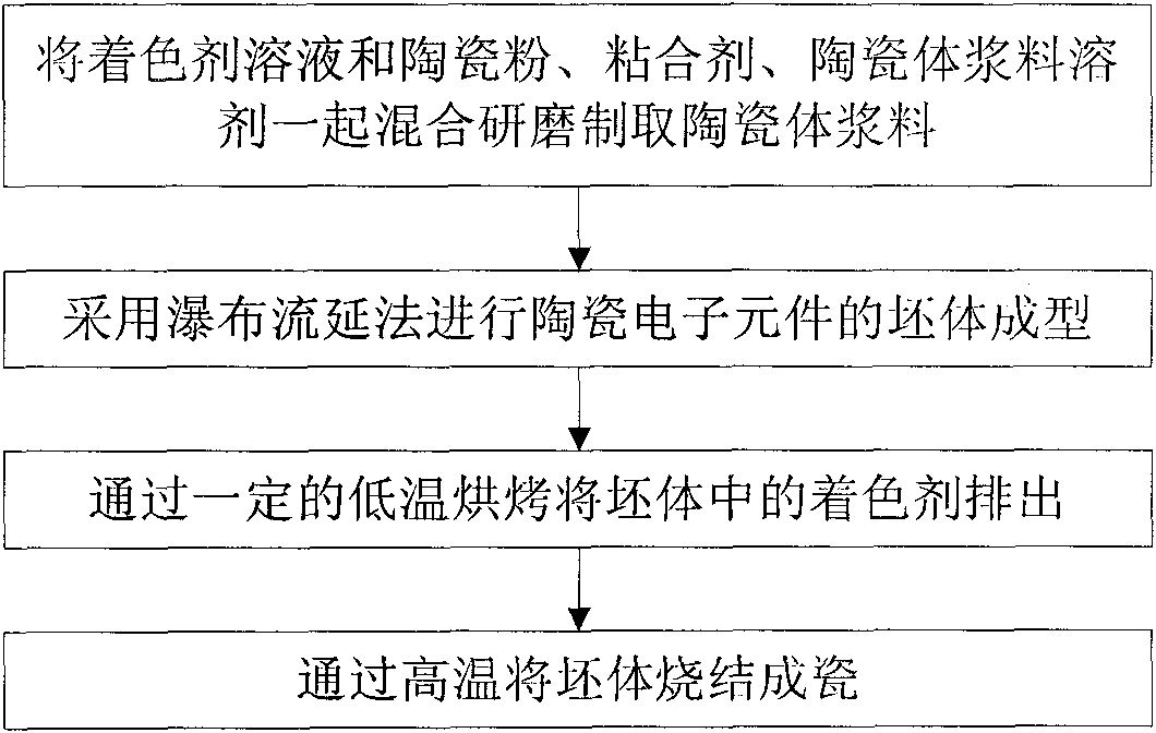
[0035] Such as figure 1 Shown is the process flow diagram of a specific embodiment of the present invention. In this embodiment, firstly, the colorant solution, ceramic powder, binder, and ceramic body slurry solvent are mixed and ground together to prepare the ceramic body slurry; The green body of ceramic electronic components is formed; then the formed green body is baked at a certain low temperature to discharge the colorant; finally, the green body is sintered into porcelain by high temperature.

Embodiment 2

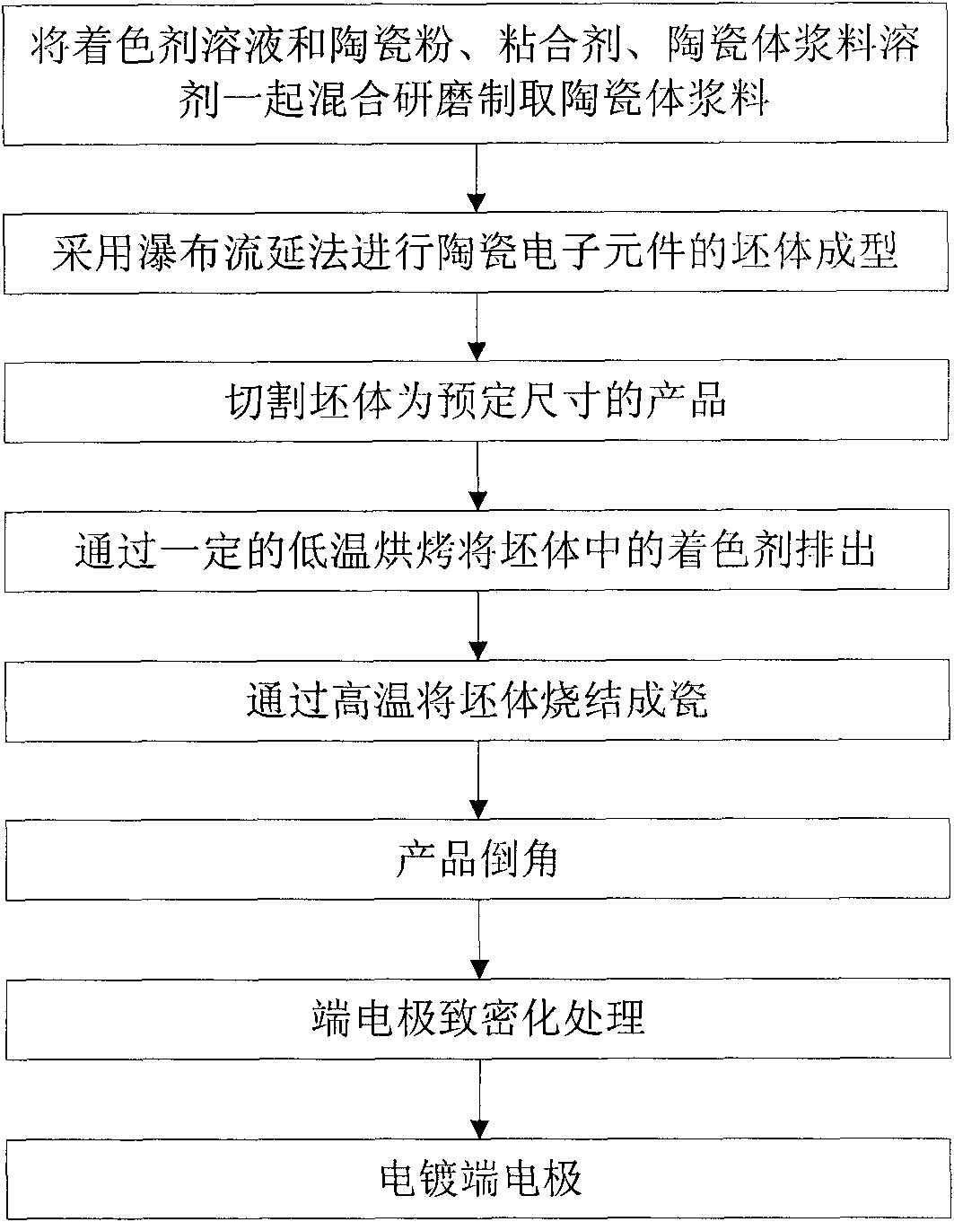
[0037] Such as figure 2 Shown, is another preferred embodiment of the present invention, and it comprises the following operation steps:

[0038] Powder making: Taking ceramic powder materials with an initial magnetic permeability of 1 as an example, first weigh a certain amount of organic colorants whose components are azo hydrocarbons (which can basically volatilize completely below 300°C) Dissolve in ethanol or other polar solvents, then filter through 325-mesh polyester gauze, filter the filtered colorant solution powder and ceramic powder, adhesive, propyl acetate and isobutanol mixed solvent or other esters and alcohols The mixed solvent and other materials are ball milled to the required size and then discharged, and the film is pulled to test the color and toughness of the diaphragm. The slurry components are as follows:

[0039] Element

ceramic body powder

binder solution

solvent

plasticizer

Colorant

Proportion

45%±0.5%

...


PUM


Abstract

The invention relates to a manufacturing method of a ceramic electronic component, which comprises the following steps: A, mixing and grinding a colorant solution with ceramic powder, a binder and a ceramic body slurry solvent together to prepare ceramic body slurry; B, printing an inner electrode and connection points, and forming a green body of the ceramic electronic component; C, discharging the colorant in the green body of the ceramic electronic component through certain low-temperature baking; and D, sintering the green body at high temperature to form the ceramic electronic component.The technical scheme of the invention can solve the problems in the prior art that the inner electrode can not be positioned easily in the printing process, the printing effect of the connection points can not be recognized easily, and products can not be accurately positioned in the cutting process, thereby improving the printing effect, the reliability of product connection and the accuracy of product cutting.

Description

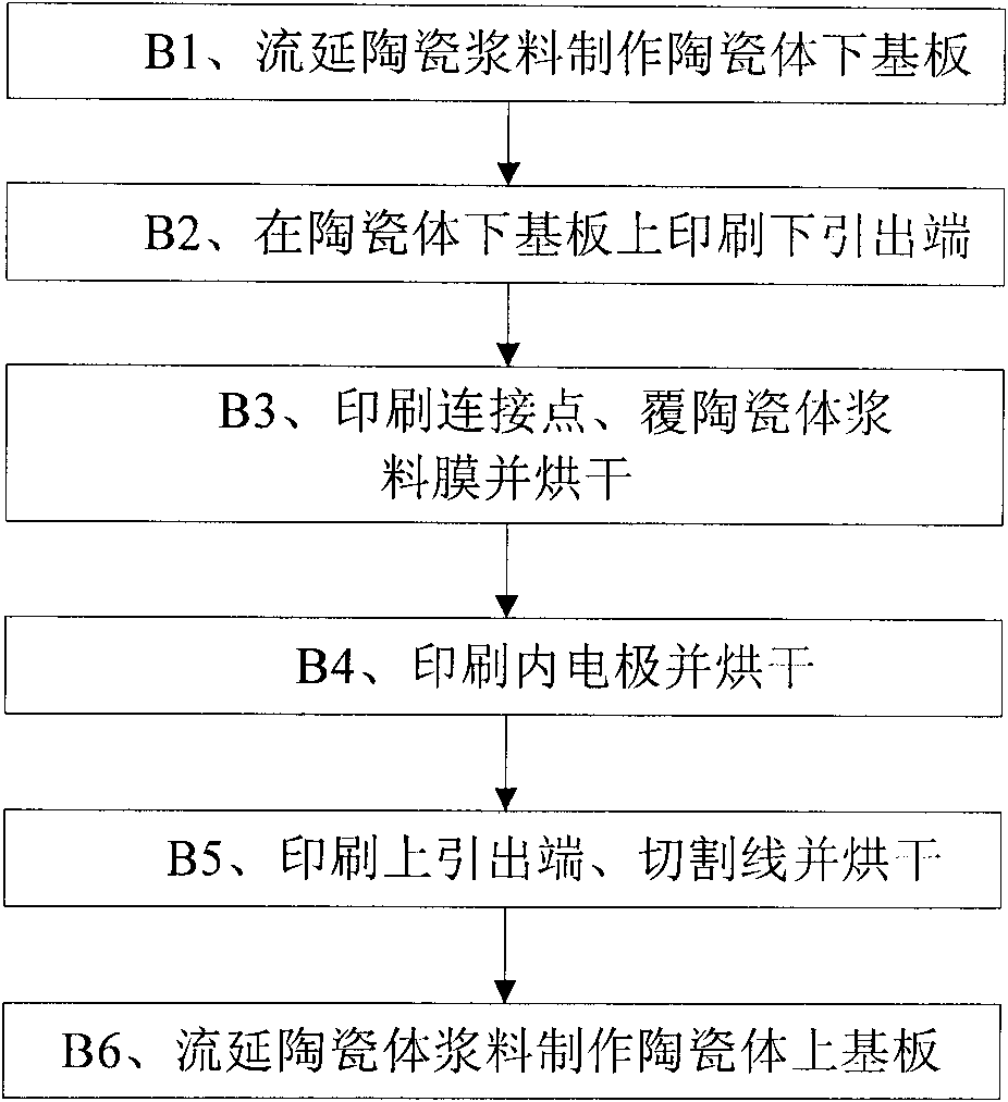
technical field [0001] The invention relates to a method for manufacturing electronic components, in particular to a method for manufacturing chip-type ceramic electronic components. Background technique [0002] Since the color of the ceramic body of the chip ceramic component is similar to the color of the internal electrode and the paste at the connection point, the production process of the chip ceramic component requires that the lower ceramic substrate be cast on the ceramic substrate first and then the electrode be printed—drying— Printing connection point (1) - cast ceramic slurry coated ceramic body film (2) - printed electrode (3)..., after such a cycle meets the design requirements, then cast the substrate, and align at (2) And the exposure of the observation point, observe the alignment effect at (1) and (3), especially the observation time at (1) should not be long, otherwise the solvent in the slurry at the connection point will volatilize, and eventually the e...

Claims


Application Information

Patent Timeline
IPC IPC(8): C04B35/622H01B17/60H01F17/00H01F41/00
Inventor 王清华曾向东张锐林
Owner SHENZHEN SUNLORD ELECTRONICS
Learn More