

Method for preparing high-density super sharp silicon probe array
A probe array, high-density technology, applied in the field of semiconductor silicon material manufacturing process
Inactive Publication Date: 2010-09-01
SHANGHAI INST OF TECHNICAL PHYSICS - CHINESE ACAD OF SCI +2
View PDF4 Cites 7 Cited by
- Summary
- Abstract
- Description
- Claims
- Application Information
AI Technical Summary
Problems solved by technology
However, almost all existing technologies require an oxide layer as a mask for secondary pattern transfer, and can only produce probe arrays with a period of more than a micron. It is still a challenge to prepare a high-density probe array with a submicron period.
Method used
View moreImage
Smart ImageViewing Examples

Examples
Embodiment 1
Embodiment 2
Embodiment 3
Login to View More PUM
 Abstract
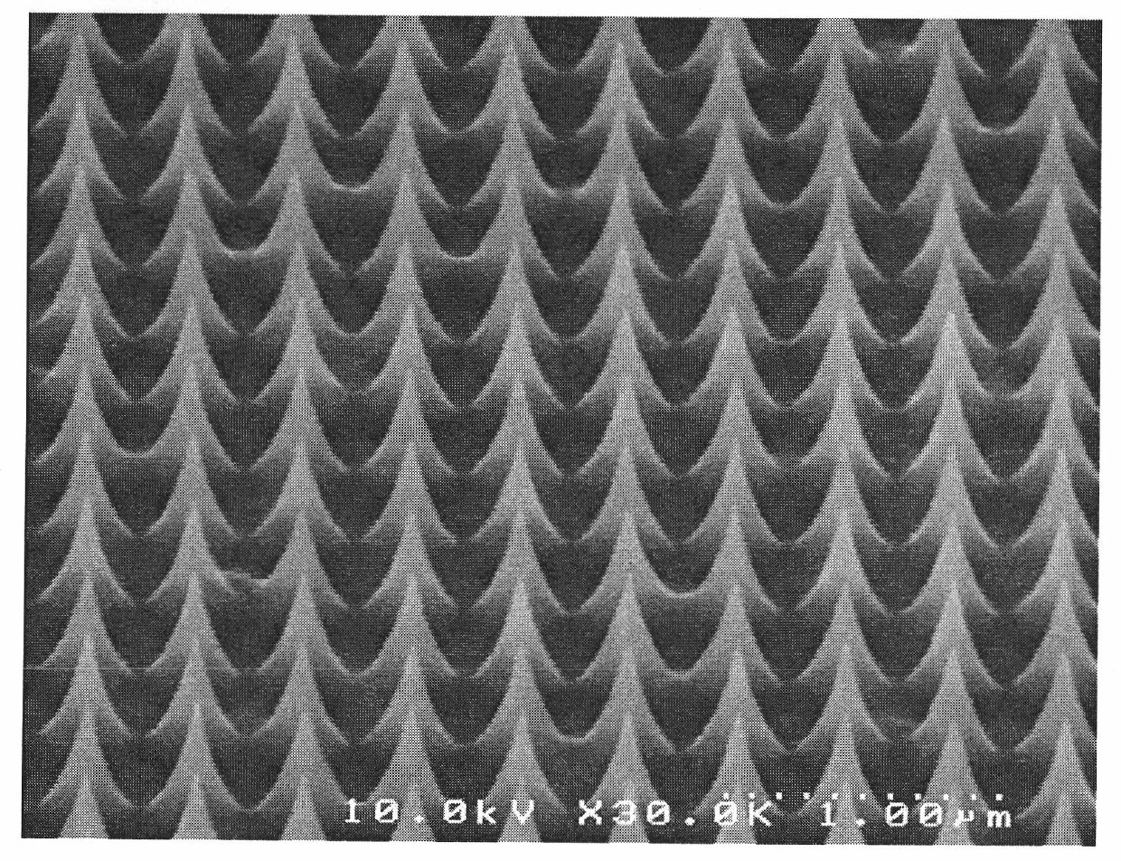
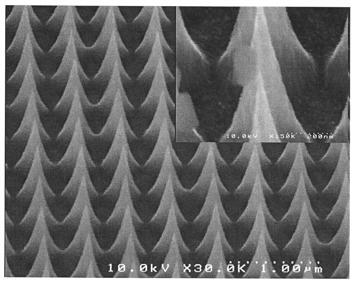
The invention provides a method for preparing a high-density super sharp silicon probe (tip) array by directly taking a hydrogen silsesquioxane (HSQ) electron beam resist as an etching mask. The hydrogen silsesquioxane (HSQ) electron beam resist is exposed by an electron beam photoetching method, and then developed to form a raster graphics of the HSQ; the silicon is subjected to isotropic etching by directly taking the HSQ as the mask; by controlling the etching conditions, the probe tip can be sharpest and the HSQ is about to fall off or automatically falls off simultaneously; the probe tip can reach several nanometers; and the additional oxidation, corrosion and other sharpening process are not needed, so the method is very simple. The method overcomes the inconvenience that the traditional preparation method needs an oxide layer to serve as a mask for secondary graphic transfer and requires additional oxidation and etching processes to sharpen the probe, and overcomes the difficulty in preparing submicron-period high-density silicon probe array, and can easily prepare the silicon probe array with the density more than 2.5*107 / mm<2>.
Description
technical field The invention relates to a semiconductor silicon material manufacturing process technology, in particular to a method for preparing a high-density, ultra-sharp silicon tip array directly using silsesquioxide hydride (HSQ) as an etching mask. Background technique Silicon probes are widely used in field emitters and probes for atomic force microscopy (AFM), scanning probe microscopy (SPM) and related probe scanning techniques (see literature [1]), and are also used as carbon nanotubes, GaN Coatings, nanoscale diamond particles and growth templates for diamond-like films (see literature [2], [3]). There is a growing demand for supertip silicon with tip size on the order of nanometers in the above fields (see literature [4]). However, almost all existing technologies require an oxide layer as a mask for secondary pattern transfer, and can only produce probe arrays with a period of more than a micron, and it is still a challenge to prepare a high-density probe a...
Claims
Login to View More Application Information
Patent Timeline
 IPC IPC(8): G01Q60/38
Inventor王少伟陆卫陈效双俞立明
OwnerSHANGHAI INST OF TECHNICAL PHYSICS - CHINESE ACAD OF SCI