Semiconductor module and portable device

A portable device, semiconductor technology, applied in the direction of semiconductor devices, semiconductor/solid-state device manufacturing, semiconductor/solid-state device components, etc.

Inactive Publication Date: 2010-09-01
SANYO ELECTRIC CO LTD
View PDF3 Cites 77 Cited by
  • Summary
  • Abstract
  • Description
  • Claims
  • Application Information

AI Technical Summary

Problems solved by technology

In existing semiconductor modules, there is room for further improvement of connection reliability with external connection electrodes

Method used


Image

  • Semiconductor module and portable device
  • Semiconductor module and portable device
  • Semiconductor module and portable device

Examples


Embodiment approach 1

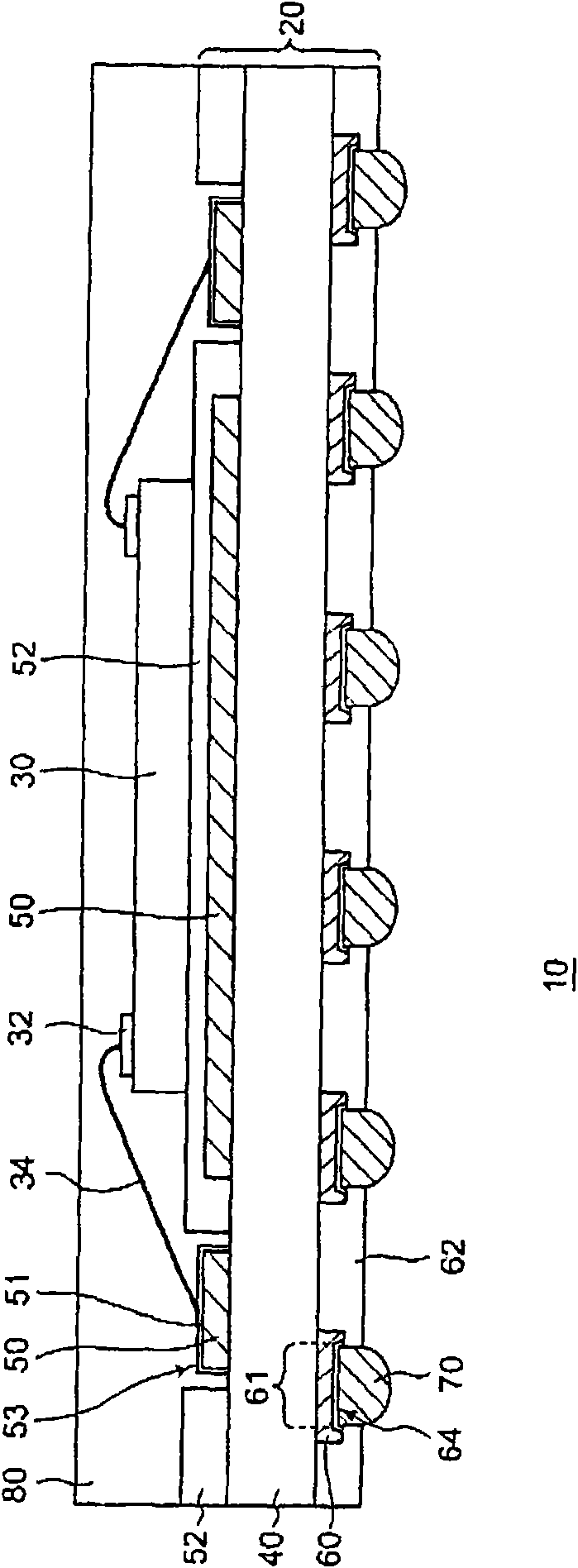
[0023] figure 1 It is a sectional view showing the structure of the semiconductor module of Embodiment 1. The semiconductor module 10 includes an element mounting substrate 20 and a semiconductor element 30 . In this embodiment, the semiconductor element 30 is connected to the element mounting substrate 20 by wire bonding.

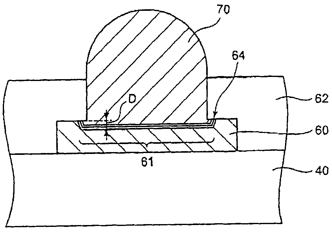
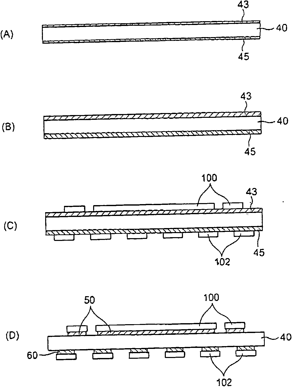
[0024] The element mounting substrate 20 includes an insulating resin layer 40, a wiring layer 50 provided on one main surface (semiconductor element mounting side) of the insulating resin layer 40, a protective layer 52, and the other main surface of the insulating resin layer 40. The wiring layer 60, the protective layer 62, and the solder ball 70.

[0025] Examples of materials constituting the insulating resin layer 40 include melamine dielectrics such as BT resins, liquid crystal polymers, epoxy resins, PPE resins, polyimide resins, fluorine-containing resins, phenolic resins, and polyamide bismaleimide. and other thermosetting resins. From the vi...

Embodiment approach 2

[0057] Figure 6 It is a sectional view showing the structure of the semiconductor module of Embodiment 2. The semiconductor module 10 of the present embodiment has a three-dimensional packaging substrate structure called a package-on-package (PoP) in which a package is mounted on a package.

[0058] In the present embodiment, the semiconductor element 30 is flip-chip connected to the element mounting substrate 20 with the electrode-formed surface facing downward.

[0059] Specifically, the wiring layer 50 includes a substrate electrode 51a for flip-chip connection and a substrate electrode 51b for stack packaging. The surface of the substrate electrode 51 a is covered with a Ni / Au layer 53 , and the element electrode 32 provided on the electrode forming surface of the semiconductor element 30 and the Ni / Au layer 53 are bonded by the solder 36 . The sealing resin 80 is provided near the semiconductor element 30 , and a part of the wiring layer 50 including the substrate elec...


PUM


Abstract

The invention provides a semiconductor module and a portable device. A wiring layer including external connection regions is provided on a main surface of an insulating resin layer on a side opposite to that of a semiconductor device mounting face. The wiring layer is coated with a protection layer. An opening is provided to the protection layer such that each external connection region is exposed. Each external connection region has a curved surface recessed toward the insulating resin layer side. The entire area of each opening is filled with a solder ball for mounting a substrate, and the recess of each external connection region is filled with the solder ball, thereby connecting each solder ball to the intermediate layer.

Description

technical field [0001] The present invention relates to a semiconductor module in which a semiconductor element is mounted on an element mounting substrate including a base and a wiring layer, and a portable device in which the semiconductor module is mounted. Background technique [0002] In the process of accelerated high-functioning of portable electronic devices such as mobile phones, PDAs, DVCs, and DSCs, in order for these products to be accepted by the market, they must be miniaturized / lightweight. In order to achieve miniaturization / lightweight, highly integrated systems are required LSI. On the other hand, these electronic devices are required to be easier to use and more convenient, and LSIs used in the devices are required to have higher functionality and higher performance. Therefore, with the high integration of LSI chips, the number of I / Os (the number of input and output parts) has increased, and on the other hand, the demand for miniaturization of the packag...

Claims


Application Information

Patent Timeline
Patent Type & Authority Applications(China)
IPC IPC(8): H01L23/498H01L23/488H01L23/373
CPCH01L2924/01032H01L2924/01046H01L2924/0105H01L2924/01082H01L23/3128H01L2924/01004H01L21/4846H01L2224/13109H01L2924/15311H01L2924/01029H01L2224/13099H01L2924/01028H01L2224/48091H01L2924/01083H01L2924/014H01L2924/01013H01L2224/484H01L24/48H01L2924/0103H01L24/45H01L2924/15331H01L2224/48599H01L2924/01047H01L2924/01079H01L23/498H01L24/13H01L24/16H01L2224/48227H01L2924/14H01L2924/01076H01L2924/01005H01L2924/01033H01L2924/01006H01L23/49816H01L2924/01078H01L2224/48228H01L2924/01011H01L2224/131H01L2224/45144H01L2924/01012H01L2224/85444H01L2224/16225H01L2924/01051H01L2224/13111H01L2924/01031H01L2224/04042H01L2224/0554H01L2224/0557H01L2224/05571H01L2224/05573H01L2224/48644H01L2924/00014H01L2924/181H01L2924/351H01L2924/01044H01L2924/00H01L2924/00012H01L2224/05599H01L2224/0555H01L2224/0556
Inventor 长松正幸小原泰浩臼井良辅
Owner SANYO ELECTRIC CO LTD
Why Eureka
Try Eureka