Method for manufacturing black silicon material

A technology of black silicon and silicon wafers, applied in the field of semiconductor optoelectronic materials

Inactive Publication Date: 2010-09-08
INST OF SEMICONDUCTORS - CHINESE ACAD OF SCI
View PDF1 Cites 20 Cited by
  • Summary
  • Abstract
  • Description
  • Claims
  • Application Information

AI Technical Summary

Problems solved by technology

[0005] The different depth of action between long-wavelength and short-wavelength laser light sources and silicon materials cannot be taken care of by using a single short-wavelength laser light source or using a single long-wavelength laser light source

Method used


Image

  • Method for manufacturing black silicon material
  • Method for manufacturing black silicon material

Examples


Embodiment Construction

[0023] In order to make the object, technical solution and advantages of the present invention clearer, the present invention will be described in further detail below in conjunction with specific embodiments and with reference to the accompanying drawings.

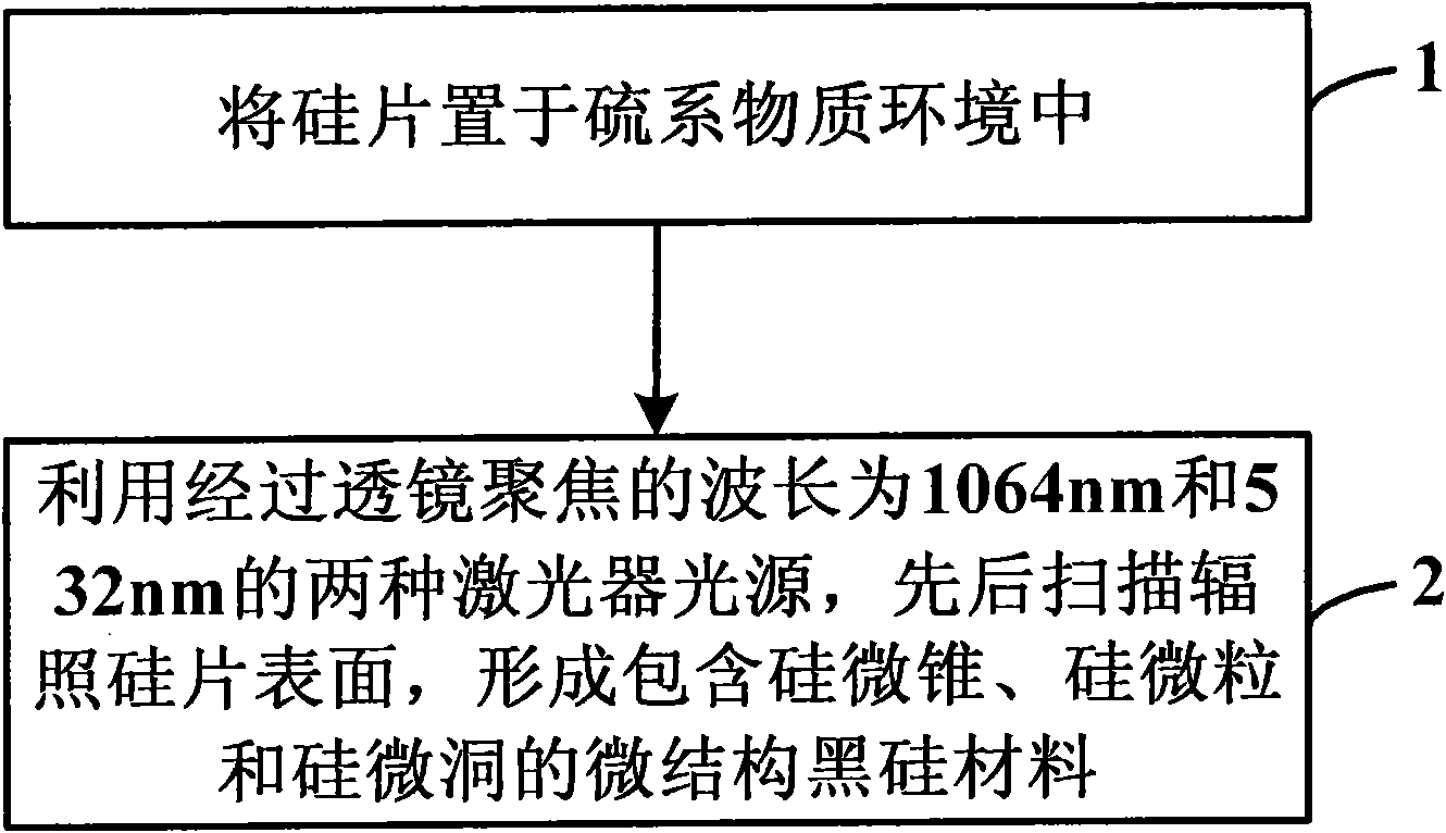
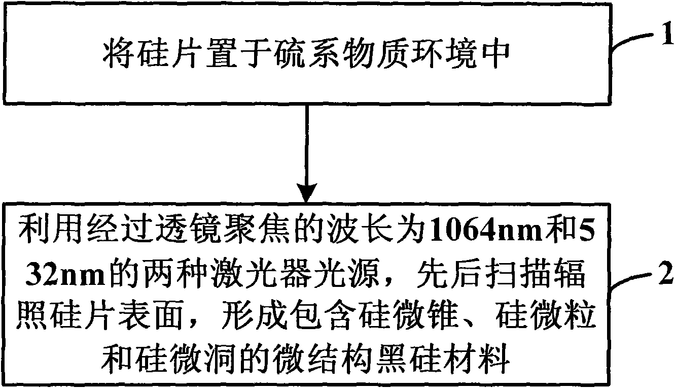
[0024] The method provided by the present invention utilizes two kinds of laser light sources with wavelengths of 1064nm and 532nm to scan and produce black silicon material, and the pulse width of the laser used is several hundred femtoseconds to several hundred nanoseconds. Place the silicon wafer in the environment of chalcogenides, scan and irradiate the silicon surface with two kinds of laser light sources with wavelengths of 1064nm and 532nm respectively, and integrate the characteristics of long-wave light source with deep action length and short-wave light source with shallow action depth into the production of black silicon materials , forming a microstructure of silicon microcones, silicon particles and silicon m...


PUM

PropertyMeasurementUnit
lengthaaaaaaaaaa
widthaaaaaaaaaa
heightaaaaaaaaaa

Abstract

The invention discloses a method for manufacturing a black silicon material by utilizing the scanning of two laser light sources with the respective wavelengths of 1064nm and 532nm, which comprises the following steps: 1. placing a silicon sheet in a sulfur series substance environment; 2. sequentially scanning and irradiating the surface of the silicon sheet by utilizing the two laser light sources which are focused through a lens and respectively have the wavelengths of 1064nm and 532nm to form the microstructural black silicon material containing silicon microcones, silicon particulates and silicon microholes. The invention simultaneously integrates the characteristics that the action depth of the long-wave light source is deep and the action depth of the short-wave light source is shallow into the manufacture of the black silicon material and expands the ranges of a sulfur series doping substance, the silicon microcones, the silicon particulates and the silicon microholes on a surface layer, so that incident light can be more fully absorbed, and the absorption coefficient of the total solar spectrum is increased to more than 90 percent.

Description

technical field [0001] The invention relates to the technical field of semiconductor optoelectronic materials, in particular to a method for making black silicon materials by scanning two kinds of laser light sources with wavelengths of 1064nm and 532nm. Background technique [0002] In recent years, material surface processing technology based on high-intensity laser irradiation has received extensive attention. Researchers at Harvard University in the United States scanned the silicon surface with a high-intensity femtosecond laser light source, and obtained a new material with a fine-sized pyramid-conical microstructure, the so-called black silicon material. [0003] The light absorption efficiency of black silicon material is significantly improved (MRS Belletin, 31 (2006) 594). Especially when silicon wafers are exposed to chalcogenide gases such as SF 6 , H 2 Under S and other environments, the black silicon material obtained after laser light source scanning has an...

Claims


Application Information

Patent Timeline
Patent Type & Authority Applications(China)
IPC IPC(8): C30B33/00C30B31/20H01L31/0288H01L31/102
Inventor 朱洪亮梁松韩培德林学春王宝华
Owner INST OF SEMICONDUCTORS - CHINESE ACAD OF SCI
Why Eureka
Try Eureka