Module, wiring board and module manufacturing method

A manufacturing method and wiring board technology, applied in the direction of final product manufacturing, printed circuit manufacturing, sustainable manufacturing/processing, etc., to achieve the effect of achieving yield and realizing workability

Inactive Publication Date: 2010-09-08
THE FUJIKURA CABLE WORKS LTD
View PDF1 Cites 4 Cited by
  • Summary
  • Abstract
  • Description
  • Claims
  • Application Information

AI Technical Summary

Problems solved by technology

However, in the case of the above-mentioned other methods, after bonding the above-mentioned electrodes, it is necessary to fill the gap between the semiconductor element and the printed wiring board with sealing resin.

Method used


Image

  • Module, wiring board and module manufacturing method
  • Module, wiring board and module manufacturing method
  • Module, wiring board and module manufacturing method

Examples


no. 1 Embodiment approach

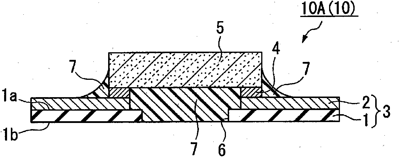
[0085] image 3 It is a cross-sectional view schematically showing a module 10A ( 10 ) according to the first embodiment of the present invention. This module 10 is roughly constituted by a wiring board 3 in which a pattern of a conductor 2 is formed on one surface 1 a of an insulating layer 1 , and a functional element 5 mounted on the conductor 2 with bumps 4 facing downward. An opening 6 is formed in a region of the wiring board 3 where the functional element 5 is mounted, smaller than the projected surface of the functional element 5 and inner than the portion where the electrode 4 is bonded to the conductor 2 . In addition, the gap between the functional element 5 and the wiring board 3 and the opening 6 are sealed with a sealing resin 7 .

[0086] The insulating layer 1 is made of resin such as polyimide, SiO 2 , BCB, Al 2 o 3 , crystallized glass, etc. From the viewpoint of improving the reliability of electrical characteristics and mechanical characteristics, glas...

no. 2 Embodiment approach

[0097] Figure 4 It is a cross-sectional view schematically showing a module 10B ( 10 ) according to the second embodiment of the present invention. The module 10B of this embodiment differs from the module 10A of the first embodiment in that the sealing resin 7 has a portion 7a protruding from the opening 6 toward the other surface 1b of the insulating layer 1 and extending to a larger area than the opening 6 .

[0098] As described above, since the sealing resin 7 has the portion 7a, when an external impact is applied to the module 10B, the impact is mitigated by the portion 7a, so that the resistance against the external impact is improved. Therefore, according to the module 10B of this embodiment, it is possible to provide electronic equipment and the like that are less likely to be damaged by external impacts.

[0099] Figure 5 It is a cross-sectional view schematically showing the wiring board 3 of the present invention. In the wiring board 3 of the present invention...

Embodiment 1

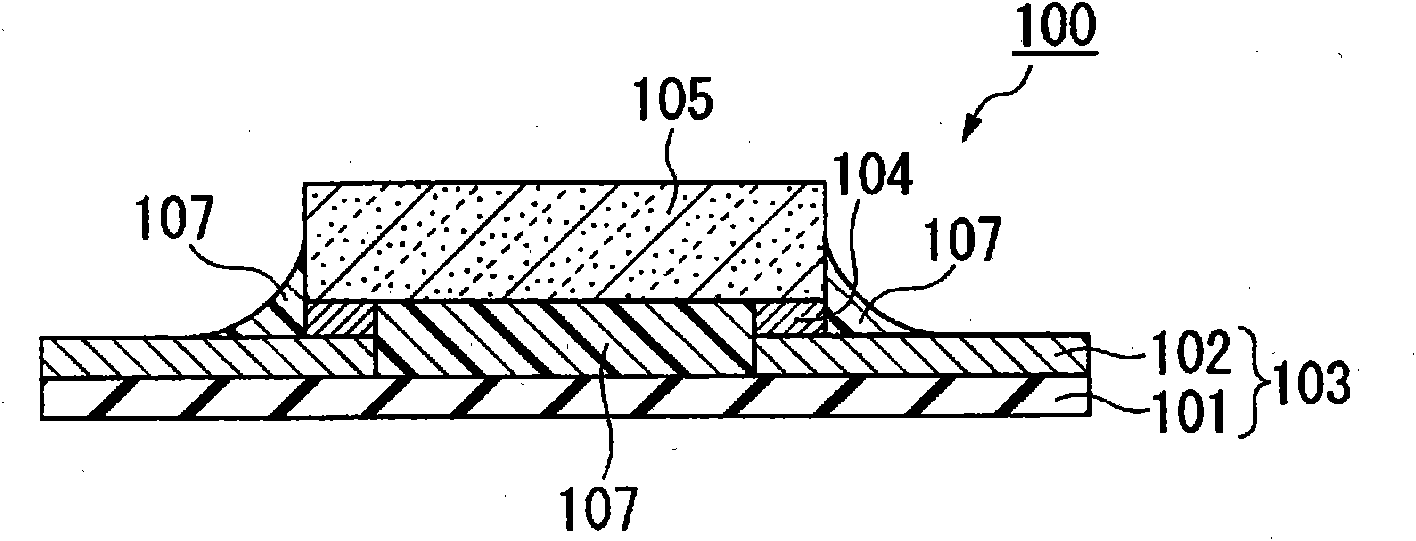
[0135] make image 3 Modules of the invention shown.

[0136] First, a printed wiring board in which a polyimide with a thickness of 40 μm was used as an insulating layer and a conductor pattern with a thickness of 18 μm was formed as a circuit was fabricated. Next, an opening of 14.5 mm×14.5 mm was formed in the position where the functional element of the insulating layer was mounted. Thereafter, a semiconductor element having an outer shape of 15 mm×15 mm and having gold bumps with a height of 15 μm formed on the electrodes was mounted on the wiring board in which the opening was formed. Next, the wiring board mounted with semiconductor components such as Figure 6A As shown, place it on a table with multiple suction holes, and pass from the suction hole to the Figure 8A Suction in the direction indicated by the arrow, and fix the wiring board on the table. Next, if Figure 8B As shown, a sealing resin having a viscosity of 1.5 Pa·s at room temperature was applied to ...


PUM

PropertyMeasurementUnit
viscosityaaaaaaaaaa
viscosityaaaaaaaaaa

Abstract

A module is provided with a wiring board wherein a conductor pattern is formed on an insulating layer, and a functional element mounted with its face down on the conductor pattern through an electrode. An opening section is formed in a region, which is in the functional element mounting position of the wiring board, is smaller than the projection surface of the functional element and is inside the portion where the electrode is bonded. A space between the functional element and the wiring board, and the opening section are sealed by a sealing resin.

Description

technical field [0001] The present invention relates to a module, a wiring board and a manufacturing method of the module, and particularly relates to a module in which functional elements are mounted on a wiring board facing downward, and the gap between the functional element and the wiring board is sealed with a sealing resin. [0002] This application claims priority based on No. 2007-259467 filed in Japan on October 3, 2007, the contents of which are incorporated herein. Background technique [0003] In recent years, the requirements for weight reduction, thinning, shortening, miniaturization, low power consumption, multi-functionality, and high reliability in electronic equipment systems have been increasing. In addition, with high integration, according to Lenz's rule (Rent's rule), functional elements such as semiconductor elements with a large number of terminals and a narrow pitch appear. [0004] On the other hand, in the process of installing these functional co...

Claims


Application Information

Patent Timeline
Patent Type & Authority Applications(China)
IPC IPC(8): H01L21/56H01L21/60
CPCH01L2924/01046H01L2224/13164H01L2924/01004H01L2924/01025H05K1/189H01L2224/13118H01L2224/81203H01L2224/16H01L2924/09701H01L2924/01322H01L2224/13116H01L2224/13144H05K2201/09072H01L2224/13147H01L2224/13099H01L2924/15151H01L2224/81805H01L2924/19041H01L2224/13124H01L21/563H05K2201/10674H01L2224/81205H01L2224/751H01L21/67126H01L2224/32225H01L2224/831H01L2924/19043H01L2224/83194H01L2924/01079H01L2224/73204H01L2224/13155H01L2224/81444H01L23/498H01L2224/13139H01L2924/14H01L2224/81411H01L2924/01078H01L2224/331H01L2224/131H05K2201/10977H05K2203/082H01L2224/16225H05K3/305H01L2224/13123H01L2224/13111H01L2924/00014H01L2924/00011Y10T29/49169Y02P70/50H01L2924/01048H01L2924/01014H01L2924/00H01L2224/0401
Inventor 伊藤彰二中谷祐介高见良大凑忠则
Owner THE FUJIKURA CABLE WORKS LTD
Why Eureka
Try Eureka